
Datasheet

MAX6001–MAX6005
Low-Cost, Low-Power, Low-Dropout,
SOT23-3 Voltage References
6 _______________________________________________________________________________________
INPUT
DYNAMIC
OUTPUT
Note 1: All devices are 100% production tested at T
A
= +25°C and are guaranteed by design for T
A
= T
MIN
to T
MAX
, as specified.
Note 2: Temperature coefficient is measured by the “box” method; i.e., the maximum ∆V
OUT
is divided by the maximum ∆t.
Note 3: Thermal hysteresis is defined as the change in +25°C output voltage before and after cycling the device from T
MIN
to T
MAX
.
Note 4: Not production tested. Guaranteed by design.
Note 5: Dropout voltage is the minimum input voltage at which V
OUT
changes ≤ 0.2% from V
OUT
at V
IN
= 5.0V (V
IN
= 5.5V for MAX6005).
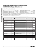
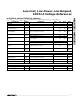
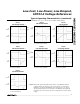
ELECTRICAL CHARACTERISTICS—MAX6005
(V
IN
= +5.5V, I
OUT
= 0, T
A
= T
MIN
to T
MAX
, unless otherwise noted. Typical values are at T
A
= +25°C.) (Note 1)
0.24 1.20Sinking: -400µA ≤ I
OUT
≤ 0
20 100
INPUT
DYNAMIC
PARAMETER SYMBOL MIN TYP MAX UNITS
Load Regulation
∆V
OUT
/
∆I
OUT
µV/µA
Line Regulation
∆V
OUT
/
∆VIN
25 240 µV/V
Output Voltage Temperature
Coefficient (Note 2)
TCV
OUT
ppm/°C
0.17 1.00
Dropout Voltage
(Note 5)
V
IN
-
V
OUT
100 200 mV
OUT Short-Circuit Current I
SC
4
mA
4
Output Voltage V
OUT
4.950 5.000 5.050 V
Temperature Hysteresis
(Note 3)
130 ppm
Long-Term Stability
∆V
OUT
/
time
50
ppm/
1,000hrs
Noise Voltage e
OUT
120 µVp-p
240 µV
RMS
Ripple Rejection
∆V
OUT
/
∆V
IN
72 dB
Turn-On Settling Time t
R
220 µs
Capacitive-Load Stability Range C
OUT
0 2.2 nF
Supply Voltage Range V
IN
V
OUT
+ 0.2 12.6 V
Quiescent Supply Current I
IN
27 45 µA
Change in Supply Current I
IN
/V
IN
0.8 2.6 µA/V
CONDITIONS
1,000 hours at T
A
= +25°C
(V
OUT
+ 0.2V) ≤ V
IN
≤ 12.6V
Sourcing: 0 ≤ I
OUT
≤ 400µA
I
OUT
= 400µA
f = 0.1Hz to 10Hz
Short to GND
Short to IN
f =10Hz to 10kHz
V
IN
= 5V ±100mV, f = 120Hz
To V
OUT
= 0.1% of final value, C
OUT
= 50pF
(Note 4)
T
A
= +25°C
Guaranteed by line-regulation test
(V
OUT
+ 0.2V) ≤ V
IN
≤ 12.6V
OUTPUT