
Datasheet
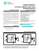

MAX6070/MAX6071
Low-Noise, High-Precision Series
Voltage References
2Maxim Integrated
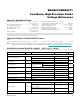
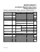
OUTF to GNDS, GNDF, GND ......................-0.3V to the lower of
(V
IN
+ 0.3V), +6V
OUTS to GNDS, GNDF, GND
.................................-0.3V to +6V
IN to GNDS, GNDF, GND
.......................................-0.3V to +6V
EN to GNDS, GNDF, GND
......................................-0.3V to +6V
FILTER to GND
............................................-0.3V to the lower of
(V
IN
+ 0.3V), +6V
GNDS to GNDF
....................................................-0.3V to +0.3V
Continuous Power Dissipation (T
A
= +70NC)
SOT23 (derate 4.3mW/NC above +70NC)
................ 347.8mW
Operating Temperature Range
........................ -40NC to +125NC
Junction Temperature
.....................................................+150NC
Storage Temperature Range
............................ -65NC to +150NC
Soldering Temperature (reflow)
......................................+260NC
Lead Temperature (soldering, 10s)
................................+300NC
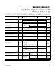
SOT23
Junction-to-Ambient Thermal Resistance (B
JA
)...........230°C/W Junction-to-Case Thermal Resistance (B
JC
)....................76°C/W
ABSOLUTE MAXIMUM RATINGS
Note 1: Package thermal resistances were obtained using the method described in JEDEC specification JESD51-7, using a four-layer
board. For detailed information on package thermal considerations, refer to www.maximintegrated.com/thermal-tutorial.
Stresses beyond those listed under “Absolute Maximum Ratings” may cause permanent damage to the device. These are stress ratings only, and functional opera-
tion of the device at these or any other conditions beyond those indicated in the operational sections of the specifications is not implied. Exposure to absolute
maximum rating conditions for extended periods may affect device reliability.
PACKAGE THERMAL CHARACTERISTICS (Note 1)
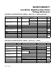
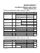
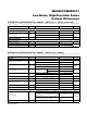
ELECTRICAL CHARACTERISTICS—MAX607__AUT12 (V
OUT
= 1.250V)
(V
IN
= +5.0V, I
OUT
= 0mA, C
OUT
= 0.1FF, T
A
= -40NC to +125NC, unless otherwise noted. Typical values are at T
A
= +25NC.) (Note 2)
PARAMETER SYMBOL CONDITIONS MIN TYP MAX UNITS
OUTPUT
Output Voltage Accuracy
MAX6070A/MAX6071A, T
A
= +25NC
-0.04 +0.04
%
MAX6070B/MAX6071B, T
A
= +25NC
-0.08 +0.08
Output Voltage Temperature
Drift (Note 3)
TCV
OUT
MAX6070A/MAX6071A 1.5 6
ppm/
NC
MAX6070B/MAX6071B 2.0 8
Line Regulation
Over specified V
IN
range
T
A
= +25NC
13 100
FV/V
T
A
= T
MIN
to T
MAX
125
Load Regulation
0mA < I
OUT
< 10mA, sink 70 150
FV/mA
0mA < I
OUT
< 10mA, source 100 150
Output Current I
OUT
-10 +10 mA
Short-Circuit Current I
SC
Sourcing to ground 25
mA
Sinking from V
IN
25
Long-Term Stability 1000 hours at T
A
= +25°C 35 ppm
Thermal Hysteresis (Note 5) 85 ppm
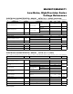
DYNAMIC CHARACTERISTICS
Noise Voltage e
OUT
1/f noise, 0.1Hz to 10Hz, C
OUT
= 0.1FF
3.6
FV
P-P
MAX6071 thermal noise, 10Hz to 10kHz,
C
OUT
= 0.1FF
5.0
FV
RMS
MAX6070 thermal noise, 10Hz to 10kHz,
C
OUT
= 0.1FF, C
FILTER
= 0.1FF
2.5
Ripple Rejection Frequency = 60Hz 100 dB