
Datasheet
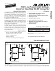
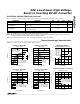
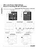

MAX629
28V, Low-Power, High-Voltage,
Boost or Inverting DC-DC Converter
2 _______________________________________________________________________________________
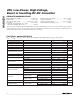
ABSOLUTE MAXIMUM RATINGS
ELECTRICAL CHARACTERISTICS
(V
CC
= +5V, C
REF
= 0.1µF, T
A
= -40°C to +85°C, unless otherwise noted. Typical values are at T
A
= +25°C.) (Note1)
Stresses beyond those listed under “Absolute Maximum Ratings” may cause permanent damage to the device. These are stress ratings only, and functional
operation of the device at these or any other conditions beyond those indicated in the operational sections of the specifications is not implied. Exposure to
absolute maximum rating conditions for extended periods may affect device reliability.
Supply Voltage (V
CC
to GND)..................................-0.3V to +6V
SHDN to GND...........................................................-0.3V to +6V
ISET, REF, FB, POL to GND.......................-0.3V to (V
CC
+ 0.3V)
LX to GND ..............................................................-0.3V to +30V
Continuous Power Dissipation (T
A
= +70°C)
SO (derate 5.88mW/°C above +70°C)..........................471mW
Operating Temperature Range ...........................-40°C to +85°C
Junction Temperature......................................................+150°C
Storage Temperature Range.............................-65°C to +165°C
Lead Temperature (soldering, 10sec).............................+300°C
CONDITIONS
V2.7 5.5V
CC
Input Voltage (Note 2)
UNITSMIN TYP MAXPARAMETER
V
FB
= 1.3V µA80 120V
CC
Supply Current
100mV hysteresis V2.3 2.5 2.65V
CC
Undervoltage Lockout
SHDN = GND
µA0.04 1V
CC
Shutdown Current
A
0.39 0.45 0.51
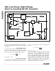
Circuit of Figure 2
V
LX
= 28V, T
A
= +85°C µA0.05 2.5LX Leakage Current
POL = GND
µs
0.7 1.0 1.3
Minimum LX Off-Time
µs6.5 8.5 10.0Maximum LX On-Time
0.20 0.25 0.33
LX Switch-Current Limit
V28Positive Output Voltage
POL = GND, V
FB
< 1V 3.0 4.5 6.0
POL = V
CC
2.0 3.2 3.8
POL = GND
(positive output)
V
1.218 1.282
1.225 1.250 1.275
nA5 50FB Input Bias Current
1.225 1.250 1.275
V
CC
= 5V
Ω
0.6 1.2
V
CC
= 3.3V 0.7 1.4
LX On-Resistance
T
A
= 0°C to +85°C
T
A
= -40°C to +85°C
T
A
= 0°C to +85°C
T
A
= -40°C to +85°C
POL = V
CC
(negative output)
mV
-25 25
FB Set Point
-15 0 15
V
CC
= 2.7V to 5.5V,
no load on REF
V
1.218 1.282
REF Output Voltage
T
A
= 0°C to +85°C
T
A
= -40°C to +85°C
V
IH
V
2.4
SHDN, POL, ISET Logic Levels
V
IL
0.4
Voltage applied to L1 (V
IN
) V
0.8
V
OUT
Input Supply Voltage (Note 2)
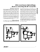
Circuit of Figure 3 V
-
V
IN
-28
Negative Output Voltage
ISET = V
CC
ISET = GND
POL = V
CC,
V
FB
> 0.25V 3.0 4.5 6.0