
Datasheet

MAX629
28V, Low-Power, High-Voltage,
Boost or Inverting DC-DC Converter
_______________________________________________________________________________________ 9
increasing usable battery life. Using separate supplies
for V
CC
and V
IN
also reduces noise injection onto V
CC
by isolating it from the switching transients, allowing a
smaller, less-expensive input filter capacitor to be used
in many applications. If input voltages below 2V will be
common, reducing the inductor to 22µH may improve
performance in this voltage range, at the potential cost
of some decrease in maximum load current and effi-
ciency.
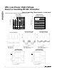
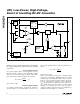
In the negative configuration shown in Figure 3, the
inverting charge pump injects current into LX with each
cycle. The amount of charge injected increases at
higher V
IN
, and may prematurely trip the internal current-
limit threshold. Resistor R3 increases the usable input
voltage range by limiting the peak injected current. The
2Ω resistor shown provides a usable input voltage
range beyond V
IN
= 15V. In applications with a different
input voltage range, R3 may be increased or
decreased as necessary, with a resulting efficiency
change of roughly 0.5%/Ω.
Layout Considerations
Proper PC board layout is essential due to high current
levels and fast switching waveforms that radiate noise.
It is recommended that initial prototyping be performed
using the MAX629 evaluation kit or equivalent PC
board-based design. Breadboards or proto-boards
should never be used when prototyping switching reg-
ulators.
It is important to connect the GND pin, the input
bypass-capacitor ground lead, and the output filter-
capacitor ground lead to a single point (star ground
configuration) to minimize ground noise and improve
regulation. Also, minimize lead lengths to reduce stray
capacitance, trace resistance, and radiated noise, with
preference given to the feedback circuit, the ground
circuit, and LX. Place R1 and R2 as close to the feed-
back pin as possible. Place the input bypass capacitor
as close as possible to V
CC
and GND.
Refer to the MAX629 evaluation kit data sheet for an
example of proper board layout.
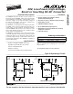
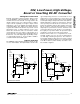
Figure 4. Adjustable Output Voltage
MAX629
V
OUT
V
BIAS
R2
( ) ARE FOR NEGATIVE OUTPUT VOLTAGE CONFIGURATIONS.
R
B
R1
FB
GND
(REF)