
Datasheet


1ppm/°C, Low-Noise, +2.5V/+4.096V/+5V
Voltage References
ABSOLUTE MAXIMUM RATINGS
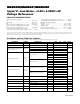
ELECTRICAL CHARACTERISTICS—MAX6325
(V
IN
= +10V, I
OUT
= 0mA, T
A
= T
MIN
to T
MAX
, unless otherwise noted. Typical values are at T
A
= +25°C.)
Stresses beyond those listed under “Absolute Maximum Ratings” may cause permanent damage to the device. These are stress ratings only, and functional
operation of the device at these or any other conditions beyond those indicated in the operational sections of the specifications is not implied. Exposure to
absolute maximum rating conditions for extended periods may affect device reliability.
(Voltages Referenced to GND)
IN ................................................................................-0.3V to 40V
OUT, TRIM..................................................................-0.3V to 12V
NR.................................................................................-0.3V to 6V
OUT Short-Circuit to GND Duration (V
IN
≤ 12V)..........Continuous
OUT Short-Circuit to GND Duration (V
IN
≤ 40V) ........................5s
OUT Short-Circuit to IN Duration (V
IN
≤ 12V) ..............Continuous
Continuous Power Dissipation (T
A
= +70°C)
8-Pin Plastic DIP (derate 9.09mW/°C above +70°C) ......727mW
8-Pin SO (derate 5.88mW/°C above +70°C)...................471mW
8-Pin CERDIP (derate 8.00mW/°C above +70°C)...........640mW
Operating Temperature Ranges
MAX63_ _ C_ A.......................................................0°C to +70°C
MAX63_ _ E_ A....................................................-40°C to +85°C
MAX63_ _ MJA ..................................................-55°C to +125°C
Storage Temperature Range ..............................-65°C to +150°C
Lead Temperature (soldering, 10s)...................................+300°C
Load Regulation (Note 2)
∆V
OUT
/
∆I
OUT
ppm/mA
+25°C
+25°C
µs5+25°Ct
ON
Turn-On Settling Time To ±0.01% of final value
µV
RMS
1.3 2.8+25°C
e
n
Output Noise Voltage (Note 3)
µVp-p1.5
mV±15 ±25C, E, M∆V
OUT
Trim-Adjustment Range
mA
3.0C, E, M
I
IN
Supply Current
1.8 2.7+25°C
10 30M
17
10Hz ≤ f ≤ 1kHz
E
0.1Hz ≤ f ≤ 10Hz
(Figure 1)
16C
ppm/
1000hr
315M
30+25°C
17
∆V
OUT
/tLong-Term Stability
E
16C
+25°CTemperature Hysteresis ppm20(Note 4)
10M
8E
7C
25+25°C
10V ≤ V
IN
≤ 36V
45M
35E
30C
MAX6325MJA 1.0 2.5M
8V ≤ V
IN
≤ 10V
CONDITIONS
MAX6325E_A
MAX6325C_A
MAX6325
ppm/V
10 18+25°C
∆V
OUT
/
∆
V
IN
Line Regulation (Note 2)
ppm/°C0.75 1.5ETCV
OUT
Output Voltage Temperature
Coefficient (Note 1)
0.5 1.0C
Output Voltage V
OUT
2.499 2.500 2.501 V
T
A
C, E, M
PARAMETER SYMBOL MIN TYP MAX UNITS
Input Voltage Range V
IN
836V
Sourcing: 0mA ≤ I
OUT
≤ 15mA
Sinking: -15mA ≤ I
OUT
≤ 0mA
MAX6325/MAX6341/MAX6350
2
Maxim Integrated
MAX6325/MAX6341/MAX6350