
Datasheet

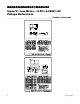

1ppm/°C, Low-Noise, +2.5V/+4.096V/+5V
Voltage References
_______________Detailed Description
Temperature Stability
The MAX6325/MAX6341/MAX6350 are highly stable,
low-noise voltage references that use a low-power tem-
perature-compensation scheme to achieve laboratory-
standard temperature stability. This produces a nearly
flat temperature curve, yet does not require the power
associated with heated references.
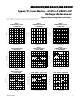
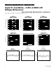
The output voltage can be trimmed a minimum of 0.6%
by connecting a 10kΩ potentiometer between OUT and
GND, and connecting its tap to the TRIM pin, as shown
in Figure 1. The external trimming does not affect tem-
perature stability.
Noise Reduction
To augment wideband noise reduction, add a 1µF
capacitor to the NR pin (Figure 2). Larger values do not
improve noise appreciably (see Typical Operating
Characteristics).
Noise in the power-supply input can affect output
noise, but can be reduced by adding an optional
bypass capacitor to the IN pin and GND.
Bypassing
The MAX6325/MAX6341/MAX6350 are stable with
capacitive load values from 0µF to 100µF, for all values
of load current. Adding an output bypass capacitor can
help reduce noise and output glitching caused by load
transients.
__________Applications Information
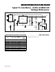
Negative Regulator
Figure 3 shows how both a +5V and -5V precision ref-
erence can be obtained from a single, unregulated +5V
supply. A MAX865 generates approximately ±9V to
operate the MAX6350 reference and MAX400 inverting
amplifier. The +5V is inverted by the ultra-low offset
MAX400 op amp. Resistor R1 is optional, and may be
used to trim the ±5V references. R2 and R4 should be
matched, both in absolute resistance and temperature
coefficient. R3 is optional, and is adjusted to set the -5V
reference.
_____________________Pin Description
NAME FUNCTION
1, 7, 8 I.C.
Internally Connected. Do not use.
2 IN Positive Power-Supply Input
PIN
4 GND Ground
3 NR
Noise Reduction. Optional capacitor
connection for wideband noise
reduction. Leave open if not used
(Figure 2).
6 OUT Voltage Reference Output
5 TRIM
External Trim Input. Allows ±1%
output adjustment (Figure 1).
Leave open if not used.
MAX6325
MAX6341
MAX6350
IN
8V TO 36V INPUT
REFERENCE OUT
OUT
TRIM
10kΩ
NR
GND
MAX6325
MAX6341
MAX6350
IN
8V TO 36V INPUT
REFERENCE OUT
OUT
TRIM
NR
*OPTIONAL
*
1µF
GND
Figure 1. Output Voltage Adjustment Figure 2. Noise-Reduction Capacitor
MAX6325/MAX6341/MAX6350
8
Maxim Integrated
MAX6325/MAX6341/MAX6350