
Datasheet

a negative-going pulse applied to V
CC
, starting above
the actual reset threshold and ending below it by the
magnitude indicated (reset comparator overdrive). The
graph indicates the typical maximum pulse width a neg-
ative-going V
CC
transient may have without causing a
reset pulse to be issued. As the magnitude of the tran-
sient increases (goes farther below the reset threshold),
the maximum allowable pulse width decreases. A 0.1µF
capacitor mounted as close as possible to V
CC
provides
additional transient immunity.
Ensuring a Valid RESET
Output Down to V
CC
= 0V
The MAX6381–MAX6390 are guaranteed to operate
properly down to V
CC
= 1V. In applications that require
valid reset levels down to V
CC
= 0V, a pulldown resistor
to active-low outputs (push/pull only, Figure 2) and a
pullup resistor to active-high outputs (push/pull only)
will ensure that the reset line is valid while the reset out-
put can no longer sink or source current. This scheme
does not work with the open-drain outputs of the
MAX6383/MAX6386/MAX6389/MAX6390. The resistor
value used is not critical, but it must be small enough
not to load the reset output when V
CC
is above the
reset threshold. For most applications, 100kΩ is ade-
quate.
MAX6381–MAX6390
SC70/µDFN, Single/Dual Low-Voltage,
Low-Power µP Reset Circuits
7
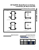
MAX6387
MAX6388
MAX6389
RESET IN
( ) IS FOR MAX6388
R1
R2
RESET
(RESET)
GND
V
CC
V
IN
MAX6381
MAX6384
MAX6387
V
CC
R1
100k
RESET
GND
Figure 1. RESET IN Configuration
Figure 2. RESET Valid to V
CC
= Ground Circuit
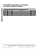
PART
RESET
THRESHOLD
RESET TIMEOUT
46
44
31
29
26
23
22
17
MAX638_
16
D3
46
44
31
29
26
23
22
17
MAX6390
16
D4
Standard Versions
Reset Timeout Delay
SUFFIX MIN
D1 1ms
D2 20ms
D3 140ms
D5 280ms
D6 560ms
D4 1120ms
D7 1200ms
MAX6390_ _D4 1120/140ms*
MAX6390_ _D7 1200/150ms*
*
The MAX6390 has a 1120ms or 1200ms RESET timeout and a
140ms or 150ms manual reset timeout.