
Datasheet
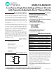


Low-Power, Single/Dual-Voltage µP Reset Circuits
with Capacitor-Adjustable Reset Timeout Delay
MAX6412–MAX6420
2
Maxim Integrated
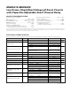
ABSOLUTE MAXIMUM RATINGS
ELECTRICAL CHARACTERISTICS
(V
CC
= 1V to 5.5V, T
A
= T
MIN
to T
MAX
, unless otherwise specified. Typical values are at V
CC
= 5V and T
A
= +25°C.) (Note 1)
Stresses beyond those listed under “Absolute Maximum Ratings” may cause permanent damage to the device. These are stress ratings only, and functional
operation of the device at these or any other conditions beyond those indicated in the operational sections of the specifications is not implied. Exposure to
absolute maximum rating conditions for extended periods may affect device reliability.
All Voltages Referenced to GND
V
CC
........................................................................-0.3V to +6.0V
SRT, MR, RESET IN....................................-0.3V to (V
CC
+ 0.3V)
RESET, RESET (Push-Pull) .........................-0.3V to (V
CC
+ 0.3V)
RESET (Open-Drain) .............................................-0.3V to +6.0V
Input Current (All Pins) .....................................................±20mA
Output Current (RESET, RESET) ......................................±20mA
Continuous Power Dissipation (T
A
= +70°C)
5-Pin SOT23 (derate 7.1mW/°C above +70°C)............571mW
Operating Temperature Range .........................-40°C to +125°C
Junction Temperature......................................................+150°C
Storage Temperature Range .............................-65°C to +150°C
Lead Temperature (soldering, 10s) .................................+300°C
Soldering Temperature (reflow)
Lead(Pb)-free packages..............................................+260°C
Packages containing lead (Pb)....................................+240°C
PARAMETER SYMBOL CONDITIONS MIN TYP MAX UNITS
Supply Voltage Range V
CC
1.0 5.5 V
V
CC
≤ 5.0V 2.6 4.5
V
CC
≤ 3.3V 2 3.5Supply Current I
CC
V
CC
≤ 2.0V 1.7 2.5
µA
T
A
= +25°C
V
TH
-
1.25%
V
TH
+
1.25%
V
CC
Reset Threshold Accuracy V
TH
T
A
= -40°C to +125°C
V
TH
-
2.5%
V
TH
+
2.5%
V
Hysteresis V
HYST
4 x V
TH
mV
V
CC
to Reset Delay t
RD
V
CC
falling at 1mV/µs 100 µs
C
SRT
= 1500pF 3.00 4.375 5.75
Reset Timeout Period t
RP
C
SRT
= 0F 0.275
ms
V
SRT
Ramp Current I
RAMP
V
SRT
= 0 to 0.65V; V
CC
= 1.6V to 5V 240 nA
V
SRT
Ramp Threshold V
TH-RAMP
V
CC
= 1.6V to 5V (V
RAMP
rising) 0.65 V
RAMP Threshold Hysteresis V
RAMP
falling threshold 33 mV
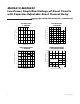
V
CC
≥ 1.0V, I
SINK
= 50µA 0.3
V
CC
≥ 2.7V, I
SINK
= 1.2mA 0.3RESET Output Voltage LOW V
OL
V
CC
≥ 4.5V, I
SINK
= 3.2mA 0.4
V
V
CC
≥ 1.8V, I
SOURCE
= 200µA 0.8 x V
CC
V
CC
≥ 2.25V, I
SOURCE
= 500µA 0.8 x V
CC
RESET Output Voltage HIGH,
(Push-Pull)
V
OH
V
CC
≥ 4.5V, I
SOURCE
= 800µA 0.8 x V
CC
V
RESET Output Leakage Current,
(Open-Drain)
I
LKG
V
CC
> V
TH
, reset not asserted 1.0 µA
V
CC
≥ 1.0V, I
SOURCE
= 1µA 0.8 x V
CC
V
CC
≥ 1.8V, I
SOURCE
= 150µA 0.8 x V
CC
V
CC
≥ 2.7V, I
SOURCE
= 500µA 0.8 x V
CC
RESET Output Voltage HIGH V
OH
V
CC
≥ 4.5V, I
SOURCE
= 800µA 0.8 x V
CC
V