
Datasheet
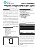


Low-Power, Single/Dual-Voltage µP Reset Circuits
with Capacitor-Adjustable Reset Timeout Delay
MAX6412–MAX6420
9
Maxim Integrated
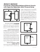
Layout Consideration
SRT is a precise current source. When developing the
layout for the application, be careful to minimize board
capacitance and leakage currents around this pin.
Traces connected to SRT should be kept as short as
possible. Traces carrying high-speed digital signals
and traces with large voltage potentials should be rout-
ed as far from SRT as possible. Leakage current and
stray capacitance (e.g., a scope probe) at this pin
could cause errors in the reset timeout period. When
evaluating these parts, use clean prototype boards to
ensure accurate reset periods.
RESET IN is a high-impedance input, which is typically
driven by a high-impedance resistor-divider network
(e.g., 1MΩ to 10MΩ). Minimize coupling to transient sig-
nals by keeping the connections to this input short. Any
DC leakage current at RESET IN (e.g., a scope probe)
causes errors in the programmed reset threshold.
Chip Information
TRANSISTOR COUNT: 325
PROCESS: BiCMOS
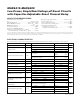
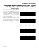
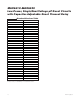
Table 1. Reset Voltages Suffix Table
SUFFIX MIN TYP MAX
16 1.536 1.575 1.614
17 1.623 1.665 1.707
18 1.755 1.800 1.845
19 1.853 1.900 1.948
20 1.950 2.000 2.050
21 2.048 2.100 2.153
22 2.133 2.188 2.243
23 2.313 2.313 2.371
24 2.340 2.400 2.460
25 2.438 2.500 2.563
26 2.559 2.625 2.691
27 2.633 2.700 2.768
28 2.730 2.800 2.870
29 2.852 2.925 2.998
30 2.925 3.000 3.075
31 2.998 3.075 3.152
32 3.120 3.200 3.280
33 3.218 3.300 3.383
34 3.315 3.400 3.485
35 3.413 3.500 3.558
36 3.510 3.600 3.690
37 3.608 3.700 3.793
38 3.705 3.800 3.895
39 3.803 3.900 3.998
40 3.900 4.000 4.100
41 3.998 4.100 4.203
42 4.095 4.200 4.305
43 4.193 4.300 4.408
44 4.266 4.375 4.484
45 4.388 4.500 4.613
46 4.509 4.625 4.741
47 4.583 4.700 4.818
48 4.680 4.800 4.920
49 4.778 4.900 5.023
50 4.875 5.000 5.125