
Datasheet


MAX6495–MAX6499
72V, Overvoltage-Protection Switches/
Limiter Controllers with an External MOSFET
11
Maxim Integrated
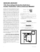
• The overvoltage waveform period (t
OV
)
• The power dissipated across the package (P
DISS
)
During an initial overvoltage occurrence, the discharge
time (Δt
1
) of C
OUT
, caused by I
OUT
and I
GATEPD
. The
discharge time is approximately:
where V
OV
is the overvoltage threshold, I
OUT
is the load
current, and I
GATEPD
is the GATE’s 100mA pulldown
current.
Upon OUT falling below the threshold point, the
MAX6495/MAX6496/MAX6499s’ charge-pump current
must recover and begins recharging the external GATE
voltage. The time needed to recharge GATE from -V
D
to
the MOSFET’s gate threshold voltage is:
where C
ISS
is the MOSFET’s input capacitance,
V
GS(TH)
is the MOSFET’s gate threshold voltage, V
D
is
the internal clamp (from OUTFB to GATE) diode’s for-
ward voltage (1.5V, typ) and I
GATE
is the charge-pump
current (100µA typ).
During Δt
2
, C
OUT
loses charge through the output load.
The voltage across C
OUT
(ΔV
2
) decreases until the
MOSFET reaches its V
GS(TH)
threshold and can be
approximated using the following formula:
Once the MOSFET V
GS(TH)
is obtained, the slope of the
output-voltage rise is determined by the MOSFET Q
g
charge through the internal charge pump with respect
to the drain potential. The new rise time needed to
reach a new overvoltage event can be calculated using
the following formula:
where Q
GD
is the gate-to-drain charge.
The total period of the overvoltage waveform can be
summed up as follows:
Δt
OV =
Δt
1
+ Δt
2
+ Δt
3
The MAX6495/MAX6496/MAX6499 dissipate the most
power during an overvoltage event when I
OUT
= 0. The
maximum power dissipation can be approximated
using the following equation:
The die-temperature increase is related to θ
JC
(8.3°C/W
and 8.5°C/W for the MAX6495/MAX6496/MAX6499,
respectively) of the package when mounted correctly
with a strong thermal contact to the circuit board. The
MAX6495/MAX6496/MAX6499 thermal shutdown is
governed by the equation:
T
J
= T
A
+ P
DISS
(θ
JC
+θ
CA
) < +170°C
Based on these calculations, the parameters of the
MOSFET, the overvoltage threshold, the output load
current, and the output capacitors are external vari-
ables affecting the junction temperature. If these para-
meters are fixed, the junction temperature can also be
affected by increasing Δt
3
, which is the time the switch
is on. By increasing the capacitance at the GATE pin,
Δt
3
increases as it increases the amount of time
required to charge up this additional capacitance
(75µA gate current). As a result, Δt
OV
increases, there-
by reducing the power dissipated (P
DISS
).
PV I
t
t
DISS OV GATEPD
OV
. =× × ×0 975
1
Δ
Δ
Δ
Δ
t
Q
V
V
I
GD
GS
OUT
GATE
3
≅
Δ
Δ
VI
t
C
OUT
OUT
2
2
=
ΔtC
VV
I
ISS
GS TH D
GATE
2
()
=
+
ΔtC
V
II
OUT
OV
OUT GATEPD
1
005
.
( )
=
×
+
Δt
2
Δt
1
GATE
OUTFB
Δt
OV
Δt
3
Figure 5. MAX6495/MAX6496/MAX6499 Timing