
Datasheet


MAX6495–MAX6499
72V, Overvoltage-Protection Switches/
Limiter Controllers with an External MOSFET
7
Maxim Integrated
Detailed Description
Overvoltage Monitoring
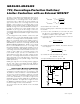
When operating in overvoltage mode, the MAX6495–
MAX6499 feedback path (Figure 1) consists of IN,
OVSET’s internal comparator, the internal gate charge
pump, and the external n-channel MOSFET, resulting in
a switch-on/off function. When the programmed over-
voltage threshold is tripped, the internal fast compara-
tor turns off the external MOSFET, clamping GATE to
OUTFB within 0.5µs and disconnecting the power
source from the load. When IN decreases below the
adjusted overvoltage threshold, the MAX6495–MAX6499
slowly enhance GATE above OUTFB, reconnecting the
load to the power source.
Overvoltage Limiter
(MAX6495/MAX6496/MAX6499)
When operating in overvoltage-limiter mode, the
MAX6495/MAX6496/MAX6499 feedback path (Figure 2)
consists of OUTFB, OVSET’s internal comparator, the
internal gate charge pump, and the external n-channel
MOSFET, resulting in the external MOSFET operating
as a voltage regulator.
During normal operation, GATE is enhanced 10V above
OUTFB. The external MOSFET source voltage is moni-
tored through a resistive divider between OUTFB and
OVSET. When OUTFB rises above the adjusted over-
voltage threshold, an internal comparator sinks the
charge-pump current, discharging the external GATE,
regulating OUTFB at the OVSET overvoltage threshold.
OUTFB remains active during the overvoltage transients
and the MOSFET continues to conduct during the over-
voltage event, operating in switched-linear mode.
As the transient begins decreasing, OUTFB fall time will
depend on the MOSFET’s GATE charge, the internal
charge-pump current, the output load, and the tank
capacitor at OUTFB.
For fast-rising transients and very large-sized MOSFETs,
add an additional bypass capacitor from GATE to GND to
reduce the effect of the fast-rising voltages at IN. The
external capacitor acts as a voltage-divider working
against the MOSFET’s drain-to-gate capacitance. For a
6000pF gate-to-source capacitance, a 0.1µF capacitor at
GATE will reduce the impact of the fast-rising V
IN
input.
Caution must be exercised when operating the
MAX6495/MAX6496/MAX6499 in voltage-limiting mode
for long durations. If the V
IN
is a DC voltage greater than
the MOSFET’s maximum gate voltage, the MOSFET dis-
sipates power continuously. To prevent damage to the
external MOSFET, proper heatsinking should be imple-
mented.
GATE Voltage
The MAX6495–MAX6499 use a high-efficiency charge
pump to generate the GATE voltage. Upon V
IN
exceed-
ing the 5V (typ) UVLO threshold, GATE enhances 10V
above V
IN
(for V
IN
≥ 14V) with a 100µA pullup current.
An overvoltage condition occurs when the voltage at
OVSET goes above its V
TH+
threshold. When the
threshold is crossed, GATE falls to OUTFB within 0.5µs
with a 100mA pulldown current. The MAX6495–MAX6499
include an internal clamp to OUTFB that ensures GATE
is limited to 18V (max) above OUTFB to prevent gate-
to-source damage of the external MOSFET.
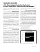
OVSET
GND
GATE
IN OUTFB
R1
V
IN
V
OUT
R2
MAX6495–
MAX6499
Figure 1. Overvoltage Threshold (MAX6495–MAX6499)
OVSET
GND
GATE
IN OUTFB
R1
C
OUT
V
IN
V
OUT
R2
MAX6495
MAX6496
MAX6499
Figure 2. Overvoltage-Limiter Protection Switch Configuration