
Datasheet


Terminal Voltage (with respect to GND)
V
DD
.......................................................................-0.3V to +6V
TS1, TS0, OUT.......................................-0.3V to (V
DD
+ 0.3V)
Input/Output Current, All Pins............................................±20mA
Continuous Power Dissipation (T
A
= +70°C)
6-pin SOT23 (derate 7.10mW/°C above +70°C)..........571mW
Operating Temperature Range...........................-40°C to +125°C
Storage Temperature Range..............................-65°C to +150°C
Lead Temperature (soldering, 10sec)...............................+300°C
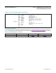
(V
DD
= +2.7V to +5.5V, T
A
= -40°C to +125°C, unless otherwise noted. Typical values are specified at T
A
= +25°C and V
DD
= +5V,
unless otherwise noted.)
Note 1: See the Temperature Accuracy histograms in the Typical Operating Characteristics.
Note 2: The output duty cycle is guaranteed to be 50% by an internal flip-flop.
PARAMETER SYMBOL CONDITIONS MIN TYP MAX UNITS
V
DD
Range V
DD
2.7 5.5 V
Supply Current I
DD
V
DD
= 5.5V
T
A
= -40°C to +85°C 140 250
µA
T
A
= -40°C to +125°C 400
Temperature Sensor
Error (Note 1)
MAX6576
T
A
= -20°C -7.5 ±1.1 +7.5
°C
T
A
= 0°C -5.5 ±0.9 +5.5
T
A
= +25°C -3.0 ±0.8 +3.0
T
A
= +85°C -4.5 ±0.5 +4.5
T
A
= +125°C -5.0 ±0.5 +5.0
MAX6577
T
A
= -20°C -7.5 ±1.1 +7.5
°C
T
A
= 0°C -6.5 ±0.9 +6.5
T
A
= +25°C -3.0 ±0.8 +3.0
T
A
= +85°C -3.5 ±0.5 +3.5
T
A
= +125°C -4.5 ±0.5 +4.5
Output Clock Period t
OUT
MAX6576,
T (temp) in °K,
Figure 1
V
TS1
= GND, V
TS0
= GND 10T
µs
V
TS1
= GND, V
TS0
= V
DD
40T
V
TS1
= V
DD
, V
TS0
= GND 160T
V
TS1
= V
DD
, V
TS0
= V
DD
640T
Output Clock Frequency f
OUT
MAX6577,
T (temp) in °K,
Figure 2
V
TS1
= GND, V
TS0
= GND 4T
Hz
V
TS1
= GND, V
TS0
= V
DD
1T
V
TS1
= V
DD
, V
TS0
= GND T/4
V
TS1
= V
DD
, V
TS0
= V
DD
T/16
OUT Duty Cycle (Note 2) 0.5
Time-Select Pin Logic Levels
V
IL
0.8
V
V
IH
2.3
OUT Voltage
V
OL
V
DD
> 4.5V, I
SINK
= 3.2mA 0.4
V
V
DD
> 2.7V, I
SINK
= 1.2mA 0.3
V
OH
V
DD
> 4.5V, I
SRC
= 800μA V
DD
- 1.5
V
DD
> 2.7V, I
SRC
= 500μA 0.8V
DD
MAX6576/MAX6577 SOT Temperature Sensors with
Period/Frequency Output
www.maximintegrated.com
Maxim Integrated
│
2
Absolute Maximum Ratings
Stresses beyond those listed under “Absolute Maximum Ratings” may cause permanent damage to the device. These are stress ratings only, and functional operation of the device at these
or any other conditions beyond those indicated in the operational sections of the specifications is not implied. Exposure to absolute maximum rating conditions for extended periods may affect
device reliability.
Electrical Characteristics