
Datasheet

CONDITIONS
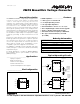
MAX660
CMOS Monolithic Voltage Converter
2 _______________________________________________________________________________________
Supply Voltage (V+ to GND, or GND to OUT) .......................+6V
LV Input Voltage ...............................(OUT - 0.3V) to (V+ + 0.3V)
FC and OSC Input Voltages........................The least negative of
(OUT - 0.3V) or (V+ - 6V) to (V+ + 0.3V)
OUT and V+ Continuous Output Current..........................120mA
Output Short-Circuit Duration to GND (Note 1) ....................1sec
Continuous Power Dissipation (T
A
= +70°C)
Plastic DIP (derate 9.09mW/°C above + 70°C) ............727mW
SO (derate 5.88mW/°C above +70°C)..........................471mW
CERDIP (derate 8.00mW/°C above +70°C)..................640mW
Operating Temperature Ranges
MAX660C_ _ ........................................................0°C to +70°C
MAX660E_ _ .....................................................-40°C to +85°C
MAX660MJA ...................................................-55°C to +125°C
Storage Temperature Range............................... -65°to +160°C
Lead Temperature (soldering, 10sec) ........................... +300°C
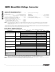
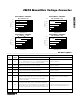
ELECTRICAL CHARACTERISTICS
(V+ = 5V, C1 = C2 = 150µF, test circuit of Figure 1, FC = open, T
A
= T
MIN
to T
MAX
, unless otherwise noted.) (Note 2)
Stresses beyond those listed under “Absolute Maximum Ratings" may cause permanent damage to the device. These are stress ratings only, and functional
operation of the device at these or any other conditions beyond those indicated in the operational sections of the specifications is not implied. Exposure to
absolute maximum rating conditions for extended periods may affect device reliability.
ABSOLUTE MAXIMUM RATINGS
Note 2: In the test circuit, capacitors C1 and C2 are 150µF, 0.2Ω maximum ESR, aluminum electrolytics.
Capacitors with higher ESR may reduce output voltage and efficiency. See Capacitor Selection section.
Note 3: Specified output resistance is a combination of internal switch resistance and capacitor ESR. See Capacitor Selection section.
Note 4: The ESR of C1 = C2 ≤ 0.5Ω. Guaranteed by correlation, not production tested.
Note 1: OUT may be shorted to GND for 1sec without damage, but shorting OUT to V+ may damage the device and should be
avoided. Also, for temperatures above +85°C, OUT must not be shorted to GND or V+, even instantaneously, or device
damage may result.
Doubler, LV = OUT
Inverter, LV = GND
Inverter, LV = open
I
L
= 100mA to GND
R
L
= 500Ω connected between OUT and GND
FC = open
T
A
≤ +85°C
R
L
= 1kΩ connected between V+ and OUT
FC = V+
T
A
≤ +85°C, C1 = C2 = 150µF
T
A
≤ +85°C, C1 = C2 = 10µF, FC = V+ (Note 4)
FC = open, LV = open
FC = V+, LV = open
T
A
≤ +85°C, OUT more negative than -4V
FC = open
T
A
> +85°C, OUT more negative than -3.8V
FC = V+
%99.00 99.96No load
Voltage-Conversion
Efficiency
%
88
Power Efficiency
92 96
96 98
±8
OSC Input Current µA
±1
kHz
40 80
Oscillator Frequency
2.5 5.5
1.5 5.5
V
3.0 5.5
R
L
= 1kΩ
Operating Supply Voltage
510
12
6.5 10.0
Ω
15
I
L
= 100mAOutput Resistance (Note 3)
mA
0.12 0.5
No loadSupply Current
13
100
mA
100
Output Current
UNITSMIN TYP MAXPARAMETER