
Datasheet

Supply Voltage (V
CC
to GND) ................................ -0.3V to +6V
DOUT to GND (MAX6672) ......................................-0.3V to +6V
DOUT to GND (MAX6673) ....................... -0.3V to (V
CC
+ 0.3V)
DOUT Short to GND..................................................Continuous
ESD Protection (Human Body Model)............................ ±2000V
Continuous Power Dissipation (T
A
= +70°C)
5-Pin SC70 (derate 2.5mW/°C above +70°C). ............200mW
Operating Temperature Range ......................... -40°C to +125°C
Storage Temperature Range ............................ -65°C to +150°C
Junction Temperature ...................................................... +150°C
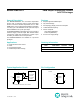
SC70 Package
Vapor Phase (60s) ...................................................... +215°C
Infrared (15s). ............................................................. +220°C
Lead Temperature (soldering, 10s) ................................ +300°C
Note 1: All specifications are 100% tested at T
A
= +25°C. Specification limits over temperature (T
A
= -40°C to +125°C) are guaranteed
by design, not production tested.
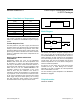
Note 2: Temperature = -200 × (0.85 - T
1
/T
2
)
3
+ (425 5 T
1
/T
2
) - 273. T
1
is the low time period. T
2
is the high time period (Figure 1).
(V
CC
= 2.4V to 5.5V, T
A
= -40°C to +125°C, unless otherwise noted. Typical values specified at +25°C and V
CC
of 3.3V.) (Note 1)
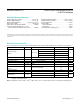
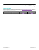
PARAMETER SYMBOL CONDITIONS MIN TYP MAX UNITS
Temperature Error
(Note 2)
V
CC
= 3.3V
T
A
= +25°C to +100°C -3 +3
°C
T
A
= 0°C to +125°C -4 +4
T
A
= -20°C to +125°C -5 +5
T
A
= -40°C to -20°C ±3
Nominal t
1
Pulse Width 280 µs
Output Low Voltage V
OL
I
SINK
= 3mA 0.4 V
Output High Voltage V
OH
I
SOURCE
= 800µA (MAX6673) V
CC
- 0.5 V
Fall Time t
FALL
C
LOAD
= 100pF 14 ns
Rise Time t
RISE
C
LOAD
= 100pF (MAX6673) 96 ns
DOUT Open-Drain Leakage
Current
V
DOUT
= 6V (MAX6672) 0.1 µA
Output Capacitance 2.5 pF
Power-Supply Rejection Ratio PSRR 2.4V to 5.5V, T
A
= -25°C to +125°C 0.3 0.8 °C/V
Supply Current I
CC
2.4V to 3.6V 60 100
µA
3.6V to 5.5V 70 150
www.maximintegrated.com
Maxim Integrated
│
2
MAX6672/MAX6673 PWM Output Temperature Sensors
in SC70 Packages
Electrical Characteristics
Stresses beyond those listed under “Absolute Maximum Ratings” may cause permanent damage to the device. These are stress ratings only, and functional operation of the device at these
or any other conditions beyond those indicated in the operational sections of the specifications is not implied. Exposure to absolute maximum rating conditions for extended periods may affect
device reliability.
Absolute Maximum Ratings