
Datasheet


Typical Applications
MAX691, MAX693, and MAX695
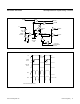
A typical connection for the MAX691/693/695 is shown
in Figure 1. CMOS RAM is powered from V
OUT
. V
OUT
is
internally connected to V
CC
when 5V power is present,
or to V
BATT
when V
CC
is less than the battery voltage.
V
OUT
can supply 50mA from V
CC
, but if more current
is required, an external PNP transistor can be added.
When V
CC
is higher than V
BATT
, the BATT ON output
goes low, providing 25mA of base drive for the external
transistor. When V
CC
is lower than V
BATT
, an internal
200Ω MOSFET connects the backup battery to V
OUT
.
The quiescent current in the battery backup mode is 1µA
maximum when V
CC
is between 0V and V
BATT
–700mV.
Reset Output
A voltage detector monitors V
CC
and generates a RESET
output to hold the microprocessor’s Reset line low when
V
CC
is below 4.65V (4.4V for MAX693). An internal
monostable holds RESET low for 50ms* after V
CC
rises
above 4.65V (4.4V for MAX693). This prevents repeated
toggling of RESET even if the 5V power drops out and
recovers with each power line cycle.
The crystal oscillator normally used to generate the clock
for microprocessors takes several milliseconds to start.
Since most microprocessors need several clock cycles
to reset, RESET must be held low until the micropro-
cessor clock oscillator has started. The MAX690 family
power-up RESET pulse lasts 50ms* to allow for this
oscillator start-up time. The manual reset switch and
the 0.1µF capacitor connected to the reset bus can be
omitted if manual reset is not needed. An inverted, active
high, RESET output is also supplied.
Power-Fail Detector
The MAX691/93/95 issues a nonmaskable interrupt (NMI)
to the microprocessor when a power failure occurs. The
+5V power line is monitored via two external resistors
connected to the power-fail input (PFI). When the volt-
age at PFI falls below 1.3V, the power-fail output (PFO)
drives the processor’s NMI input low. If a power-fail
threshold of 4.8V is chosen, the microprocessor will
have the time when V
CC
fails from 4.8V to 4.65V to save
data into RAM. An earlier power-fail warning can be
generated if the unregulated DC input of the 5V regulator
is available for monitoring.
RAM Write Protection
The MAX691/MAX693/MAX695 CE OUT line drives the
Chip Select inputs of the CMOS RAM. CE OUT follows
CE IN as long as V
CC
is above the 4.65V (4.4V for
MAX693) reset threshold. If V
CC
falls below the reset
threshold, CE OUT goes high, independent of the logic
level at CE IN. This prevents the microprocessor from
writing erroneous data into RAM during power-up, power-
down, brownouts, and momentary power interruptions.
The LOW LINE output goes low when V
CC
falls below
4.65V (4.4V for MAX693).
*200ms for MAX695
Figure 1. MAX691/693/695 Typical Application
+5V
V
CC
INPUT
NO CONNECTION
0.1µF
0.1µF
0.1µF
3
1
9
4
V
CC
V
BATT
I/O
NMI
RESET
PFI
GND
BATT ON
LOW LINE WDO
SYSTEM STATUS INDICATORS
3V
BATTERY
5
2
12
13
6 14
MAX691
MAX693
MAX695
11
10
15
7
OSC IN
V
OUT
CE IN
CE OUT
PFO
WDI
RESET
RESET
8
OSC SEL
AUDIBLE
ALARM
ADDRESS
DECODE
CMOS
RAM
MICROPROCESSOR
OTHER SYSTEM RESET SOURCES
A0-A15
MAX690–MAX695 Microprocessor Supervisory Circuits
www.maximintegrated.com
Maxim Integrated
│
6