
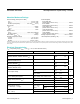
Datasheet


Detailed Description
Battery-Switchover and V
OUT
The battery switchover circuit compares V
CC
to the V
BATT
input, and connects V
OUT
to whichever is higher. Switchover
occurs when V
CC
is 50mV greater than V
BATT
as V
CC
falls,
and V
CC
is 70mV more than V
BATT
as V
CC
rises (see
Figure 4). The switchover comparator has 20mV of hyster-
esis to prevent repeated, rapid switching if V
CC
falls very
slowly or remains nearly equal to the battery voltage.
When V
CC
is higher than V
BATT
, V
CC
is internally
switched to V
OUT
via a low saturation PNP transis-
tor. V
OUT
has 50mA output current capability. Use an
external PNP pass transistor in parallel with internal tran-
sistor if the output current requirement at V
OUT
exceeds
50mA or if a lower V
CC
-V
OUT
voltage differential is
desired. The BATT ON output (MAX691/MAX693/MAX695
only) can directly drive the base of the external transistor.
It should be noted that the MAX690–MAX695 need only
supply the average current drawn by the CMOS RAM if
there is adequate filtering. Many RAM data sheets specify
a 75mA maximum supply current, but this peak current
spike lasts only 100ns. A 0.1µF bypass capacitor at V
OUT
supplies the high instantaneous current, while V
OUT
need
only supply the average load current, which is much less.
A capacitance of 0.1µF or greater must be connected to
the V
OUT
terminal to ensure stability.
A 200Ω MOSFET connects V
BATT
input to V
OUT
during
battery backup. This MOSFET has very low input-to-
output differential (dropout voltage) at the low current
levels required for battery backup of CMOS RAM or other
low power CMOS circuitry. When V
CC
equals V
BATT
the
supply current is typically 12µA. When V
CC
is between
0V and (V
BATT
- 700mV) the typical supply current is only
600nA typical, 1µA maximum.
The MAX690/MAX691/MAX694/MAX695 operate with
battery voltages from 2.0V to 4.25V while MAX692/
MAX693 operate with battery voltages from 2.0V to
4.0V. High value capacitors can also be used for short-
term memory backup. External circuitry is required to
ensure that the capacitor voltage does not rise above
the reset threshold, and that the charging resistor does
not discharge the capacitor when in backup mode. The
MAX691A and the MAX791 provide solutions requiring
fewer external components.
A small charging current of typically 10nA (0.1µA max)
flows out of the V
BATT
terminal. This current varies with the
amount of current that is drawn from V
OUT
but its polarity
is such that the backup battery is always slightly charged,
and is never discharged while V
CC
is in its operating volt-
age range. This extends the shelf life of the backup battery
by compensating for its self-discharge current. Also note
that this current poses no problem when lithium batteries
are used for backup since the maximum charging current
(0.1µA) is safe for even the smallest lithium cells.
If the battery-switchover section is not used, connect
V
BATT
to GND and connect V
OUT
to V
CC
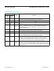
. Table 2 shows
the state of the inputs and output in the low power battery
backup mode.
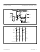
Figure 3. MAX691/MAX693/MAX695 Block Diagram
RESET GENERATOR
TIMEBASE FOR RESET
AND
WATCHDOG
WATCHDOG TRANSITION
DETECTOR
WATCHDOG
TIMER
+
-
1.3V
+
-
+
-
*
4.65V
V
BATT
BATT ON1 5
V
CC
CHIP-ENABLE INPUT
OSC IN
*4.4V (MAX693)
OSC SEL
WATCHDOG INPUT
POWER FAIL
INPUT
3
13
7
8
11
9
4
V
OUT
CHIP ENABLE OUTPUT
LOW LINE
RESET
GROUND
RESET
WATCHDOG OUTPUT
POWER FAIL OUTPUT
2
12
6
15
16
14
10
MAX690–MAX695 Microprocessor Supervisory Circuits
www.maximintegrated.com
Maxim Integrated
│
8