
Datasheet


MAX7032
Low-Cost, Crystal-Based, Programmable,
ASK/FSK Transceiver with Fractional-N PLL
2 _______________________________________________________________________________________
ABSOLUTE MAXIMUM RATINGS
Stresses beyond those listed under “Absolute Maximum Ratings” may cause permanent damage to the device. These are stress ratings only, and functional
operation of the device at these or any other conditions beyond those indicated in the operational sections of the specifications is not implied. Exposure to
absolute maximum rating conditions for extended periods may affect device reliability.
HVIN to GND .........................................................-0.3V to +6.0V
PAVDD, AVDD, DVDD to GND..............................-0.3V to +4.0V
ENABLE, T/R, DATA, CS, DIO, SCLK, CLKOUT to
GND......................................................-0.3V to (HVIN + 0.3V)
All Other Pins to GND...............................-0.3V to (_V
DD
+ 0.3V)
Continuous Power Dissipation (T
A
= +70°C)
32-Pin Thin QFN (derate 21.3mW/°C above +70°C)....1702mW
Operating Temperature Range .........................-40°C to +125°C
Storage Temperature Range .............................-65°C to +150°C
Lead Temperature (soldering, 10s) .................................+300°C
Soldering Temperature (reflow) .......................................+260°C
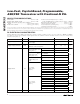
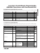
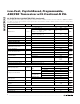
DC ELECTRICAL CHARACTERISTICS
(
Typical Application Circuit
, 50Ω system impedance, V
AVDD
= V
DVDD
= V
PAVDD
= V
HVIN
= +2.1V to +3.6V, f
RF
= 300MHz to 450MHz,
T
A
= -40°C to +125°C, unless otherwise noted. Typical values are at V
AVDD
= V
DVDD
= V
PAVDD
= V
HVIN
= +2.7V, T
A
= +25°C, unless
otherwise noted.) (Note 1)
PARAMETER SYMBOL CONDITIONS MIN TYP MAX UNITS
Supply Voltage (3V Mode) V
DD
HVIN, PAVDD, AVDD, and DVDD connected to
power supply
2.1 2.7 3.6 V
Supply Voltage (5V Mode) HVIN
PAVDD, AVDD, and DVDD unconnected from
HVIN, but connected together
4.5 5.0 5.5 V
f
RF
= 315MHz
3.5 5.4
Transmit mode, PA off,
V
DATA
at 0% duty cycle
(ASK) (Note 2)
f
RF
= 434MHz
4.3 6.7
f
RF
= 315MHz
7.6 12.3
Transmit mode, V
DATA
at 50% duty cycle
(ASK) (Notes 3, 4)
f
RF
= 434MHz
8.4 13.6
f
RF
= 315MHz (Note 4)
11.6 19.1
Transmit mode, V
DATA
at 100% duty cycle
(FSK)
f
RF
= 434MHz (Note 2)
12.4 20.4
mA
Receiver (ASK 315MHz)
6.1 7.9
Receiver (ASK 434MHz) 6.4 8.3
Receiver (FSK 315MHz) 6.4 8.4
Receiver (FSK 434MHz) 6.7 8.7
mA
DRX (3V mode) 23.4 77.3
DRX (5V mode) 67.2 94.4
Deep-sleep (3V mode) 0.8 8.8
T
A
< +85°C,
typ at +25°C
(Note 4)
Deep-sleep (5V mode) 2.4 10.9
µA
Receiver (ASK 315MHz)
6.4 8.2
Receiver (ASK 434MHz) 6.7 8.4
Receiver (FSK 315MHz) 6.8 8.7
Receiver (FSK 434MHz) 7.0 8.8
mA
DRX (3V mode) 33.5 103.0
DRX (5V mode) 82.3 116.1
Deep-sleep (3V mode) 8.0 34.2
Supply Current I
DD
T
A
< +125°C,
typ at +125°C
(Note 2)
Deep-sleep (5V mode) 14.9 39.3
µA
Voltage Regulator V
REG
V
HVIN
= 5V, I
LOAD
= 15mA 3.0 V