
Datasheet

3.3V/5V/Adjustable-Output,
Step-Up DC-DC Converters
Supply Voltage (OUT to GND) ....................................-0.3V, +7V
Switch Voltage (LX to GND) ........................................-0.3V, +7V
Auxiliary Pin Voltages (SHDN
, LBI, LBO, REF,
3/5
, FB to GND) ........................................-0.3V, (V
OUT
+ 0.3V)
Reference Current (I
REF
) ....................................................2.5mA
Continuous Power Dissipation (T
A
= +70°C)
Plastic DIP (derate 9.09mW/°C above +70°C) .............727mW
SO (derate 5.88mW/°C above +70°C)..........................471mW
Operating Temperature Ranges:
MAX75_C_ _ ........................................................0°C to +70°C
MAX75_E_ _......................................................-40°C to +85°C
Junction Temperature......................................................+150°C
Storage Temperature Range............................... -65°to +160°C
Lead Temperature (soldering, 10sec) ........................... +300°C
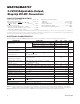
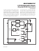
ELECTRICAL CHARACTERISTICS
(Circuits of Figure 1 and Typical Operating Circuit, V
IN
= 2.5V, I
LOAD
= 0mA, T
A
= T
MIN
to T
MAX
, unless otherwise noted.)
Stresses beyond those listed under “Absolute Maximum Ratings" may cause permanent damage to the device. These are stress ratings only, and functional
operation of the device at these or any other conditions beyond those indicated in the operational sections of the specifications is not implied. Exposure to
absolute maximum rating conditions for extended periods may affect device reliability.
ABSOLUTE MAXIMUM RATINGS
Note 1: Supply current from the 3.3V output is measured with an ammeter between the 3.3V output and OUT pin. This current
correlates directly with actual battery supply current, but is reduced in value according to the step-up ratio and efficiency.
Note 2: Minimum value is production tested. Maximum value is guaranteed by design and is not production tested.
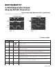
LBO Output Leakage Current
SHDN, 3/5, FB, LBI Input Current
V2.7 5.5
MAX757, I
LOAD
= 0mA (Note 2)
Output Voltage Range
V1.22 1.25 1.28MAX757FB Voltage
nA±100
LBI = 1.25V, FB = 1.25V, SHDN = 0V or 3V,
3/5 = 0V or 3V
V1.6SHDN, 3/5 Input Voltage High
V0.4SHDN, 3/5 Input Voltage Low
Shutdown Quiescent Current
(Note 1)
Battery Quiescent Current
Measured at V
IN
in Figure 1
V1.22 1.25 1.28With falling edgeLBI Input Threshold
mV25LBI Input Hysteresis
V0.4
I
SINK
= 2mA
LBO Output Voltage Low
µA1LBO = 5V
µA20 40
SHDN = 0V, LBI = 1.25V, 3/5 = 3V, V
OUT
= 3.47V,
FB = 1.3V (MAX757 only)
µA
Quiescent Supply Current in
3.3V Mode (Note 1)
MAX757, V
OUT
= 5V, 0mA < I
LOAD
< 200mA
MAX756, 3/5 = 0V, 0mA < I
LOAD
< 200mA
MAX756, 3/5 = 3V, 0mA < I
LOAD
< 300mA
%0.8 2.0
3/5 = 3V, -20µA < REF load < 250µA, C
REF
= 0.22µF
Reference-Voltage Regulation
V1.23 1.25 1.27No REF load, C
REF
= 0.1µF
60
I
LOAD
= 0mA, 3/5 = 3V, LBI = 1.25V, V
OUT
= 3.47V,
FB = 1.3V (MAX757 only)
µA
V
60Output set for 3.3V
1.1 1.8
I
LOAD
= 10mA
Minimum Start-Up Supply Voltage
4.8 5.0 5.2
2V < V
IN
< 3V
Reference Voltage
3.17 3.30 3.43 V
4.8 5.0 5.2
Output Voltage
UNITSMIN TYP MAXCONDITIONSPARAMETER
V0.7
I
LOAD
= 20mA
Minimum Operating Supply
Voltage (once started)
MAX756/MAX757
2
Maxim Integrated