
Datasheet

3.3V/5V/Adjustable-Output,
Step-Up DC-DC Converters
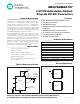
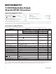
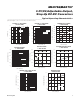
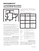
______________________________________________________________Pin Description
NAME FUNCTION
1
SHDN
2 3/5 Selects the main output voltage setting; 5V when low, 3.3V when high.
– FB
3 REF
4 LBO
5 LBI
6 OUT
7 GND Power Ground. Must be low impedance; solder directly to ground plane.
8 LX 1A, 0.5Ω N-Channel Power MOSFET Drain
1
–
2
3
4
5
6
7
8
PIN
MAX756 MAX757
Shutdown Input disables SMPS when low, but the voltage reference and low-battery com-
parator remain active.
Feedback Input for adjustable output operation. Connect to an external voltage divider
between OUT and GND.
1.25V Reference Voltage Output. Bypass with 0.22µF to GND (0.1µF if there is no external
reference load). Maximum load capability is 250µA source, 20µA sink.
Low-Battery Output. An open-drain N-channel MOSFET sinks current when the voltage at
LBI drops below +1.25V.
Low-Battery Input. When the voltage on LBI drops below +1.25V, LBO sinks current.
Connect to V
IN
if not used.
Connect OUT to the regulator output. It provides bootstrapped power to both devices,
and also senses the output voltage for the MAX756.
OUTPUT
VOLTAGE
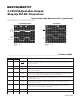
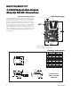
50mV/div
V
IN
= 2.5V
HORIZONTAL = 50μs/div
5V Mode
LOAD-TRANSIENT RESPONSE
OUTPUT
CURRENT
0mA to 200mA
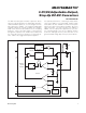
_____________________________Typical Operating Characteristics (continued)
(Circuit of Figure 1, T
A
= +25°C, unless otherwise noted.)
V
SHDN
2V/div
V
IN
= 2.5V
HORIZONTAL = 5ms/div
5V Mode
START-UP DELAY
V
OUT
2V/div
3V
0V
5V
0V
MAX756/MAX757
4
Maxim Integrated