
Datasheet

3.3V/5V/Adjustable-Output
Step-Up DC-DC Converters
3.3V/5V/Adjustable-Output,
Step-Up DC-DC Converters
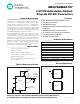
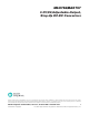
GND
GND
LBI
OUT
3/5 (MAX756)
FB (MAX757)
REF
SHDN
LX
LBO
0.122"
(3.10mm)
0.080"
(2.03mm)
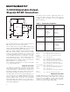
___________________Chip Topography
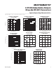
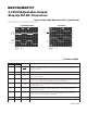
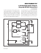
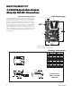
________________________________________________________Package Information
L
DIM
A
A1
B
C
D
E
e
H
h
L
α
MIN
0.053
0.004
0.014
0.007
0.189
0.150
0.228
0.010
0.016
0°
MAX
0.069
0.010
0.019
0.010
0.197
0.157
0.244
0.020
0.050
8°
MIN
1.35
0.10
0.35
0.19
4.80
3.80
5.80
0.25
0.40
0°
MAX
1.75
0.25
0.49
0.25
5.00
4.00
6.20
0.50
1.27
8°
INCHES MILLIMETERS
α
8-PIN PLASTIC
SMALL-OUTLINE
PACKAGE
HE
D
e
A
A1
C
h x 45˚
0.127mm
0.004in.
B
1.27 BSC0.050 BSC
21-325A
PC Layout and Grounding
The MAX756/MAX757 high peak currents and high-fre-
quency operation make PC layout important for mini-
mizing ground bounce and noise. The distance
between the MAX756/MAX757’s GND pin and the
ground leads of C1 and C2 in Figure 1 must be kept to
less than 0.2" (5mm). All connections to the FB and LX
pins should also be kept as short as possible. To
obtain maximum output power and efficiency and mini-
mum output ripple voltage, use a ground plane and
solder the MAX756/MAX757 GND (pin 7) directly to the
ground plane.
TRANSISTOR COUNT: 758
SUBSTRATE CONNECTED TO OUT
MAX756/MAX757
8
Maxim Integrated