
Datasheet
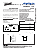

MAX8569A/MAX8569B
200mA Step-Up Converters in 6-Pin
SOT23 and TDFN
_______________________________________________________________________________________ 7
Detailed Description
The MAX8569A and MAX8569B compact high-efficien-
cy step-up converters feature low-quiescent supply cur-
rent to ensure the highest possible efficiency over a
wide load range. With a minimum 1.5V input voltage,
these devices are well suited for applications with two
alkaline cells, two nickel-metal-hydride (NiMH) cells, or
one lithium-ion (Li+) cell. When SHDN is low, the output
is connected to the battery through the inductor and an
internal p-channel MOSFET. This allows the input bat-
tery to be used as a backup or real-time clock supply
when the converter is off by eliminating the voltage drop
across the MOSFET body diode. These devices are
ideal for low-power applications where a small footprint
is critical. The internal synchronous rectifier improves
efficiency significantly and reduces size and cost by
eliminating the need for an external Schottky diode.
Control Scheme
The MAX8569A/MAX8569B feature a current-limited
control scheme that provides ultra-low quiescent current
and high efficiency over a wide output current range.
The switching cycles are not controlled by an oscillator.
Instead, switch on-time is terminated when the inductor
current reaches the 780mA (typ) n-channel current limit,
or when the 5µs maximum n-channel switch on-time is
reached. Following each on-cycle, the synchronous rec-
tifier turns on, shunts the MOSFET body diode, and the
inductor current ramps to zero before another cycle
begins. The next cycle occurs when the error compara-
tor senses that the output has fallen below the regulation
threshold.
Applications Information
Shutdown
Drive SHDN low to shut down the MAX8569A/
MAX8569B and reduce the input current to less than
1µA. During shutdown, the battery input is connected
to the output through the inductor and the internal syn-
chronous rectifier. This allows the input battery (rather
than a separate backup battery) to provide backup
power for devices such as an idled microcontroller,
SRAM, or real-time clock, without the usual diode for-
ward drop. Drive SHDN to V
OUT
(logic-high) to enable
the IC for normal operation.
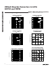
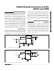
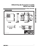
MAX8569A
FB
OUT
1.5V TO 3V
INPUT
L1
10µH
C3
22µF
C1
10µF
3.3V OUTPUT
R4
100kΩ
R3
168kΩ
LX
4
1
2
5
6
3
SHDN
BATT
GND
C2
0.01µF
R2
1MΩ
R1
220kΩ
Figure 1. Typical Application Circuit for MAX8569A
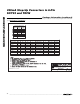
MAX8569B
OUT
1.5V TO 3V
INPUT
L1
10µH
C3
22µF
C1
10µF
3.3V
OUTPUT
RESET
OUTPUT
R1
100kΩ
LX
4
1
2
5
6
3
SHDN
BATT
GND
RST
OFF
ON
Figure 2. Typical Application Circuit for MAX8569B