
Datasheet
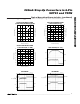
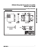

MAX8569A/MAX8569B
200mA Step-Up Converters in 6-Pin
SOT23 and TDFN
8 _______________________________________________________________________________________
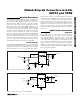
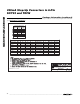
Low-Battery Cutoff
The SHDN trip threshold of the MAX8569A/MAX8569B
can be used as an input voltage detector that disables
the IC when the battery voltage falls to a set level. The
SHDN trip threshold is 1.228V. Use a resistor-divider to
set the battery-detection voltage (R1 and R2 in Figure 1).
Select R2 between 100kΩ and 1MΩ to minimize battery
drain. Calculate R1 as follows:
R1 = R2 x ((V
OFF
/ V
SHDN
) - 1)
where V
OFF
is the battery voltage at which the part
shuts down and V
SHDN
= 1.228V. Note that input ripple
can sometimes cause false shutdowns. To minimize the
effect of ripple, connect a low-value capacitor (C2)
from SHDN to GND to filter out input noise. Select a C2
value so the R1, C2 time constant is above 2ms.
Power-On Reset (
RST,
MAX8569B)
The MAX8569B provides a power-on reset output (RST)
that goes high impedance when the output reaches 90%
of its regulation point. RST pulls low when the output is
below 90% of the regulation point. Connect a 100kΩ to
1MΩ pullup resistor from RST to OUT to provide a logic
control signal for a microprocessor. Connect RST to
GND when the reset function is not used.
Setting the Output Voltage (MAX8569A)
The output of the MAX8569A is adjustable from 2V to
5.5V. Connect a resistor-divider from the output to ground
with FB connected to the center tap to set the desired
output voltage (R3 and R4, Figure 1). Select R4 between
100kΩ and 1MΩ. R3 is then calculated as follows:
R3 = R4 x ((V
OUT
/ V
FB
) - 1)
where V
OUT
is the desired output voltage and V
FB
is
1.228V.
Inductor Selection
The control scheme of the MAX8569A/MAX8569B per-
mits flexibility in choosing an inductor. A 10µH inductor
performs well for most applications, but values from
4.7µH to 100µH can be used as well. Small inductance
values typically offer smaller physical size. Output
power is reduced when the inductance is large enough
to prevent the maximum current limit (780mA) from
being reached before the maximum on-time (5µs)
expires. For maximum output current, choose L so that:
where R
L
is the inductor series resistance and R
NCH
is
the R
DS(ON)
of the internal n-channel MOSFET (0.3Ω typ).
Capacitor Selection
Choose an output capacitor to achieve the desired out-
put ripple percentage.
C
OUT
> (0.5 x L x 0.780A
2
) / (r% x V
OUT
2
)
where L is the inductor value and r is the desired output
ripple in %. A 22µF ceramic capacitor is a good start-
ing value.
The input capacitor reduces the peak current drawn
from the battery and can be the same value as the out-
put capacitor. A larger input capacitor can be used to
further reduce the input ripple and improve efficiency.
PC Board Layout and Grounding
Careful printed circuit layout is important for minimizing
ground bounce and noise. Keep the IC’s GND pin and
the ground leads of the input- and output-filter capaci-
tors less than 0.2in (5mm) apart. In addition, keep all
connections to the FB and LX pins as short as possible.
In particular, when using external feedback resistors,
locate them as close to FB as possible. To maximize
output power and efficiency and minimize output ripple
voltage, use a ground plane and solder the IC’s GND
directly to the ground plane. A sample layout is avail-
able in the MAX8569A/MAX8569B evaluation kit to
speed designs.
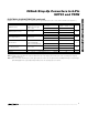
Chip Information
PROCESS: BiCMOS
Vs
A
L
Vs
A
I
A
V
A
RR
V
BATT MAX BATT MIN
OUT MAX
BATT MIN NCH L
OUT
() ()
()
()
.
.
.
.
×
<<
×
=
×−×+
()
1
078
5
078
078
2
078
2
µµ
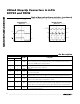
Selector Guide
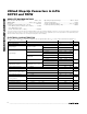
PART
OUTPUT
VOLTAGE
PIN-
PACKAGE
TOP
MARK
MAX8569AEUT
Adjustable
SOT23-6
ABWK
MAX8569BEUT
Fixed 3.3V
SOT23-6
ABWL
MAX8569AETT
Adjustable
TDFN AJN
MAX8569BETT
Fixed 3.3V
TDFN AJO
MAX8569BETT30
Fixed 3.0V
TDFN AJP