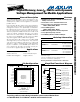
9-0587; Rev 3; 6/10 KIT ATION EVALU E L B AVAILA High-Efficiency, Low-IQ, PMICs with Dynamic Voltage Management for Mobile Applications The MAX8660/MAX8661 power management ICs (PMICs) power applications processors (APs) in smart cellular phones, PDAs, Internet appliances, and other portable devices. Four step-down DC-DC outputs, three linear regulators, and an 8th always-on LDO are integrated with powermanagement functions.
MAX8660/MAX8660A/MAX8660B/MAX8661 High-Efficiency, Low-IQ, PMICs with Dynamic Voltage Management for Mobile Applications Table of Contents General Description . . . . . . . . . . . . . . . . . . . . . . . . . . . . . . . . . . . . . . . . . . . . . . . . . . . . . . . . . . . . . . . . . . . . . . . . . . . 1 Applications . . . . . . . . . . . . . . . . . . . . . . . . . . . . . . . . . . . . . . . . . . . . . . . . . . . . . . . . . . . . . . . . . . . . . . . . . . . . . . . . . 1 Features . . . . . . .
High-Efficiency, Low-IQ, PMICs with Dynamic Voltage Management for Mobile Applications Design Procedure . . . . . . . . . . . . . . . . . . . . . . . . . . . . . . . . . . . . . . . . . . . . . . . . . . . . . . . . . . . . . . . . . . . . . . . . . . . . 38 Setting the Output Voltages . . . . . . . . . . . . . . . . . . . . . . . . . . . . . . . . . . . . . . . . . . . . . . . . . . . . . . . . . . . . . . . . 38 Inductor Selection . . . . . . . . . . . . . . . . . . . . . . . . . . . . . . . . . . . . . .
MAX8660/MAX8660A/MAX8660B/MAX8661 High-Efficiency, Low-IQ, PMICs with Dynamic Voltage Management for Mobile Applications ABSOLUTE MAXIMUM RATINGS IN, IN5, IN6, IN67, EN2, EN34, EN5, LBO, RSO, MR, SET1, SET2, V1, V2, V3, V4, SCL, SDA, SRAD to AGND..................................................-0.3V to +7.5V LBF, LBR, EN1, RAMP to AGND .................-0.3V to (VIN + 0.3V) V8 to AGND................................................-0.3V to (VIN8 + 0.3V) V5 to AGND..........................................
High-Efficiency, Low-IQ, PMICs with Dynamic Voltage Management for Mobile Applications (VIN = VIN5 = VIN67 = VIN8 = 3.6V, Figure 3, TA = -40°C to +85°C, unless otherwise noted. Typical values are at TA = +25°C.) (Note 2) PARAMETER PWM Switching Frequency SYMBOL CONDITIONS fSW MIN TYP MAX UNITS 1.9 2.0 2.
MAX8660/MAX8660A/MAX8660B/MAX8661 High-Efficiency, Low-IQ, PMICs with Dynamic Voltage Management for Mobile Applications ELECTRICAL CHARACTERISTICS (continued) (VIN = VIN5 = VIN67 = VIN8 = 3.6V, Figure 3, TA = -40°C to +85°C, unless otherwise noted. Typical values are at TA = +25°C.) (Note 2) PARAMETER SYMBOL CONDITIONS REG2—SYNCHRONOUS STEP-DOWN DC-DC CONVERTER SET2 = IN, VPV2 = 4.
High-Efficiency, Low-IQ, PMICs with Dynamic Voltage Management for Mobile Applications (VIN = VIN5 = VIN67 = VIN8 = 3.6V, Figure 3, TA = -40°C to +85°C, unless otherwise noted. Typical values are at TA = +25°C.) (Note 2) PARAMETER SYMBOL p-Channel Current-Limit Threshold ILIM3 CONDITIONS MIN TYP MAX 1.85 2.15 2.45 n-Channel Zero-Crossing Threshold n-Channel Negative Current Limit REG3 Maximum Output Current Forced-PWM mode only IOUT3 2.
MAX8660/MAX8660A/MAX8660B/MAX8661 High-Efficiency, Low-IQ, PMICs with Dynamic Voltage Management for Mobile Applications ELECTRICAL CHARACTERISTICS (continued) (VIN = VIN5 = VIN67 = VIN8 = 3.6V, Figure 3, TA = -40°C to +85°C, unless otherwise noted. Typical values are at TA = +25°C.) (Note 2) PARAMETER EN34 to V4 Enable Time SYMBOL tPHLVTH4 CONDITIONS MIN 400 MAX8660B, powering up to 1.
High-Efficiency, Low-IQ, PMICs with Dynamic Voltage Management for Mobile Applications (VIN = VIN5 = VIN67 = VIN8 = 3.6V, Figure 3, TA = -40°C to +85°C, unless otherwise noted. Typical values are at TA = +25°C.) (Note 2) PARAMETER SYMBOL LBO, RSO Output-High Leakage Current LBO Output Low Level Minimum VIN for LBO Assertion LBO Deassert Delay tVBHBFH CONDITIONS MAX UNITS VIN = 6V, TA = +25°C 0.2 µA 2.6V ≤ VIN ≤ 6V, sinking 3mA 0.2 VIN = 1V, sinking 100µA 0.
MAX8660/MAX8660A/MAX8660B/MAX8661 High-Efficiency, Low-IQ, PMICs with Dynamic Voltage Management for Mobile Applications ELECTRICAL CHARACTERISTICS (continued) (VIN = VIN5 = VIN67 = VIN8 = 3.6V, Figure 3, TA = -40°C to +85°C, unless otherwise noted. Typical values are at TA = +25°C.) (Note 2) PARAMETER SYMBOL CONDITIONS MIN TYP MAX UNITS 400 kHz I2C TIMING Clock Frequency Hold Time (Repeated) START Condition fSCL tHD;STA Figure 8 0.6 µs CLK Low Period tLOW 1.
High-Efficiency, Low-IQ, PMICs with Dynamic Voltage Management for Mobile Applications QUIESCENT CURRENT vs. INPUT VOLTAGE QUIESCENT CURRENT (µA) 80 70 60 50 40 30 20 2.5 MAX8660 toc02 SDA = SDL = V8 REG1–REG7 DISABLED REG8 IS ALWAYS ON 90 2.4 SWITCHING FREQUENCY (MHz) 100 MAX8660/61 toc01 SWITCHING FREQUENCY vs. INPUT VOLTAGE 10 2.3 2.2 2.1 2.0 1.9 1.8 1.7 1.6 0 1.5 2.5 3.0 3.5 4.0 4.5 5.0 INPUT VOLTAGE (V) 5.5 6.0 2.5 3.0 SWITCHING FREQUENCY vs. TEMPERATURE 5.5 6.
Typical Operating Characteristics (continued) (Circuit of Figure 3, VIN = 3.6V, TA = +25°C, unless otherwise noted.) 80 75 VIN = 4.2V 70 65 VIN = 3.6V 60 VIN 1V/div 3.6V 3.2 ILOAD = 1000mA 3.0 2.8 2.6 V1 = 3.3V L1 = 1.2µH (TOKO DE2812C) 55 5.0V 100mV/div V1 2.4 600mA LOAD, V1 = 3.3V 3.3V OUTPUT 2.2 50 0.01 0.1 1 10 2.5 1000 10,000 100 3.0 LOAD CURRENT (mA) 3.36 3.32 -1.5%/A 3.28 3.26 3.34 3.32 3.30 3.28 3.26 3.24 3.24 FORCED-PWM NORMAL 3.
High-Efficiency, Low-IQ, PMICs with Dynamic Voltage Management for Mobile Applications REG2 OUTPUT VOLTAGE vs. INPUT VOLTAGE REG2 EFFICIENCY vs. LOAD CURRENT 90 80 VIN = 4.2V 75 70 1.90 VIN = 3.6V 65 VIN 1V/div 3.6V 1.85 1.80 800mA LOAD 1.75 100mV/div V2 60 1.70 450mA LOAD, V2 = 1.8V V2 = 1.8V 1.65 50 1 10 100 LOAD CURRENT (mA) 2.5 1000 REG2 LOAD REGULATION 3.0 3.5 4.0 4.5 5.0 INPUT VOLTAGE (V) 5.5 6.0 40µs/div REG2 DROPOUT VOLTAGE vs. LOAD CURRENT REG2 OUTPUT VOLTAGE vs.
Typical Operating Characteristics (continued) (Circuit of Figure 3, VIN = 3.6V, TA = +25°C, unless otherwise noted.) REG3 EFFICIENCY vs. LOAD CURRENT 75 70 VIN = 4.2V 65 VIN = 3.6V 60 ILOAD = 1000mA 1.43 V3 = 1.4V L3 = 1.2µH (TOKO DE2812C) 55 MAX8660 toc26 1.44 OUTPUT VOLTAGE (V) 5.0V VIN 1V/div 3.6V 1.42 1.41 1.40 1.39 1.38 50mV/div V3 1.37 1.36 800mA LOAD, V3 = 1.4V 1.35 50 0.01 0.1 1 10 100 LOAD CURRENT (mA) 2.5 1000 10,000 REG3 LOAD REGULATION VIN = 3.6V 1.
High-Efficiency, Low-IQ, PMICs with Dynamic Voltage Management for Mobile Applications REG4 EFFICIENCY vs. LOAD CURRENT REG4 OUTPUT VOLTAGE vs. INPUT VOLTAGE 90 80 75 VIN = 4.2V 70 65 ILOAD = 300mA 1.41 OUTPUT VOLTAGE (V) EFFICIENCY (%) 85 VIN = 3.6V MAX8660 toc35 MAX8660 toc34 FORCED-PWM NORMAL REG4 LINE TRANSIENT 1.42 MAX8660 toc33 95 5.0V VIN 1.39 1.38 1.37 L4 = 4.7µH (TOKO DE2812C) 1.36 200mA LOAD, V5 = 1.4V V4 = 1.4V 50 1.35 0.1 1 10 100 LOAD CURRENT (mA) 1000 2.
Typical Operating Characteristics (continued) (Circuit of Figure 3, VIN = 3.6V, TA = +25°C, unless otherwise noted.) 1.81 1.80 1.79 1.78 100mA LOAD 1.82 OUTPUT VOLTAGE (V) 1.82 OUTPUT VOLTAGE (V) 1.82 REG5 OUTPUT VOLTAGE vs. TEMPERATURE 1.83 MAX8660 toc43 MAX8660 toc42 100mA LOAD OUTPUT VOLTAGE (V) REG5 OUTPUT VOLTAGE vs. LOAD CURRENT 1.83 1.81 1.80 1.79 1.78 1.77 3.0 3.5 4.0 4.5 5.0 INPUT VOLTAGE (V) 5.5 6.0 1.80 1.79 1.
High-Efficiency, Low-IQ, PMICs with Dynamic Voltage Management for Mobile Applications 3.0 1.80 1.79 1.86 4.2V INPUT 3.3V OUTPUT 2.5 2.0 1.5 1.78 3.5 4.0 4.5 5.0 INPUT VOLTAGE (V) 5.5 6.0 1.80 1.78 1.76 1.70 0 100 200 300 400 500 600 700 800 900 LOAD CURRENT (mA) -40 -15 10 35 TEMPERATURE (°C) 60 85 REG6/REG7 LOAD TRANSIENT REG6/REG7 LINE TRANSIENT MAX8660 toc55 MAX8660 toc54 5.0V VIN 1V/div 3.6V 50mV/div V6/V7 300mA 20mV/div V6/V7 IV6/IV7 100mA/div 10mA V6/V7 = 1.
Typical Operating Characteristics (continued) (Circuit of Figure 3, VIN = 3.6V, TA = +25°C, unless otherwise noted.) REG8 LOAD REGULATION REG8 OUTPUT VOLTAGE vs. INPUT VOLTAGE MAX8660 toc59 3.2 VIN = 3.6V 3.8 3.6 3.4 3.0 3.2 V8 (V) OUTPUT VOLTAGE (V) 4.0 MAX8660 toc58 5mA LOAD 3.4 2.8 3.0 2.8 2.6 2.6 2.4 2.4 2.2 2.2 2.0 2.0 2.5 3.0 3.5 4.0 4.5 5.0 INPUT VOLTAGE (V) 5.5 0 6.0 10 20 30 40 50 60 LOAD CURRENT (mA) 70 80 REG8 LINE TRANSIENT REG8 OUTPUT VOLTAGE vs.
High-Efficiency, Low-IQ, PMICs with Dynamic Voltage Management for Mobile Applications PIN MAX8660 MAX8661 1 1 NAME FUNCTION IN5 REG5 Power Input. Connect IN5 to IN to ensure V5 rises first to meet the Marvell PXA3xx processor’s sequencing requirements. If adherence to this sequencing specification is not required, connect IN5 to V1, V2, or another supply between 2.35V and VIN. See the Linear Regulators (REG5–REG8) section for more information. REG5 Linear-Regulator Output. V5 defaults to 1.
MAX8660/MAX8660A/MAX8660B/MAX8661 High-Efficiency, Low-IQ, PMICs with Dynamic Voltage Management for Mobile Applications Pin Description (continued) PIN MAX8660 MAX8661 FUNCTION 16 16 PG2 REG2 Power Ground. Connect PG1, PG2, PG3, PG4, and AGND together. Refer to the MAX8660 EV kit data sheet for more information. 17 17 IN8 REG8 Input Power Connection. IN8 must be connected to IN. 18 18 IN Main Battery Input. This input provides power to the IC. Connect a 0.
High-Efficiency, Low-IQ, PMICs with Dynamic Voltage Management for Mobile Applications PIN MAX8660 MAX8661 32 32 NAME FUNCTION EN2 REG2 Enable Input. Drive EN2 high to turn on REG2. EN2 has hysteresis so that an RC can be used to implement manual sequencing with respect to other inputs. EN2 is typically driven by the SYS_EN output of an Marvell PXA3xx processor. 33 33 SRAD Serial-Address Input. Connect SRAD to AGND for a 7-bit slave address of 0110 100 (0x68).
MAX8660/MAX8660A/MAX8660B/MAX8661 High-Efficiency, Low-IQ, PMICs with Dynamic Voltage Management for Mobile Applications V1 3.3V AT 1200mA 1045mA 15mA VCC_USB 5mA VCC_TSI MARVELL PXA3xx PROCESSOR AUXILIARY POWER PERIPHERALS MAX8660 10mA VCC_I01 25mA VCC_I03 50mA VCC_I04 50mA VCC_I06 55mA VCC_LCD 20mA VCC_MSL 50mA VCC_DF 35mA VCC_CI 135mA IN 160mA 200mA V2 1.8V AT 900mA 540mA VCC_MEM AUXILARY POWER PERIPHERALS MEMORY V3 0.725V TO 1.8V AT 1600mA 1600mA VCC_APPS V4 0.
High-Efficiency, Low-IQ, PMICs with Dynamic Voltage Management for Mobile Applications IN REF 1.25V PV1 TO BATT BATTERY LBF (1.20V) LBR (1.25V) UVLO OVLO AND BATT MON LX1 STEP-DOWN PWM REG1 TO ALL BLOCKS OPEN-DRAIN LOW BATT OUT TO nBATT_FAULT PG1 ON PWM LBO V1, VCC_I0x, VCC_LCD, VCC_MSL, VDD_USB, VCC_DF, VDD_CI, VCC_TSI MAX8660/MAX8660B: 3.3V, 3.0V, 2.85V MAX8660A: 2.5V, 2.0V, 1.
MAX8660/MAX8660A/MAX8660B/MAX8661 High-Efficiency, Low-IQ, PMICs with Dynamic Voltage Management for Mobile Applications 2.6V TO 6.0V INPUT R10 20Ω IN R1 1.82MΩ 18 IN C22 0.47µF IN PV1 21 36 LBF R2 80.6kΩ 22 LBR V8 C11 4.7µF U1 MAX8660 MAX8660A MAX8660B R3 1MΩ PG1 V1 19 R5 300kΩ LX1 AGND PV2 13 LBO 32 31 EN34 25 EN5 39 SET1 6 SET2 33 C21 0.1µF V8 20 V8 LX2 PG2 V2 PV3 EN5 L2 2.0µH 16 C7 10µF 10 28 L3 1.
High-Efficiency, Low-IQ, PMICs with Dynamic Voltage Management for Mobile Applications The MAX8660/MAX8661 PMICs are optimized for devices using the applications processors, including smart cellular phones, PDAs, Internet appliances, and other portable devices requiring substantial computing and multimedia capability and low power consumption. The MAX8660/MAX8661 comply with the specifications for Marvell’s PXA300 family (PXA3xx) and Marvell’s Armada 100 family (PXA16x) of processors.
MAX8660/MAX8660A/MAX8660B/MAX8661 High-Efficiency, Low-IQ, PMICs with Dynamic Voltage Management for Mobile Applications Table 2. Maxim and Marvell PXA3xx Digital Signal Terminology MAXIM MARVELL DESCRIPTION EN34 PWR_EN Active-High Enable Signal for Processor Core Power. The applications processor drives this PWR_EN signal high to exit sleep mode. The processor’s PWR_EN logic is powered by the MAX8660/MAX8661 “always on” V8 (VCC_BBATT) regulator during sleep mode.
High-Efficiency, Low-IQ, PMICs with Dynamic Voltage Management for Mobile Applications The REG2 regulator has an on-chip synchronous rectifier. See the REG1–REG4 Synchronous Rectification section for more information. The REG2 regulator allows 100% duty-cycle operation. See the REG1/REG2 100% Duty-Cycle Operation (Dropout) section for more information.
converters to maintain regulation until the input voltage falls below the desired output voltage plus the dropout voltage specification of the converter. During 100% duty-cycle operation, the high-side p-channel MOSFET turns on constantly, connecting the input to the output through the inductor.
High-Efficiency, Low-IQ, PMICs with Dynamic Voltage Management for Mobile Applications (i.e., 1.8V to 2.5V) ramp-rate control. During a positive voltage change, the output-voltage dV/dt is as fast as possible. To avoid this fast output dV/dt, disable REG6 or REG7 before changing the output. With this method, the soft-start ramp rate limits the output dV/dt, and therefore, the input current is controlled. During a negative voltage change (i.e., 2.5V to 1.
MAX8660/MAX8660A/MAX8660B/MAX8661 High-Efficiency, Low-IQ, PMICs with Dynamic Voltage Management for Mobile Applications REG3/REG4 Enable (EN34, EN3, EN4) REG3 and REG4 have independent I 2C enable bits (EN3, EN4) and a shared hardware-enable input (EN34). As shown in Figure 5, the EN34 hardwareenable input is logically ORed with the I2C enable bits. Table 6 is the truth table for the V3/V4 enable logic. Note that to achieve a pure I2C enable/disable, connect EN34 to ground.
High-Efficiency, Low-IQ, PMICs with Dynamic Voltage Management for Mobile Applications POWER MODE POWER DOMAIN STATE MAX8660 QUIESCENT OPERATING CURRENT (FIGURE 3) NORMAL FORCED-PWM OPERATING MODE MODE DIGITAL CONTROL STATE V1, V2, V3, V4, V5, V6, V7, EN1/EN2/EN5 (SYS_EN) and EN34 (PWR_EN) and V8 are on are asserted; V6, V7 are enabled by I2C V1, V2, V3, V4, V5, EN1/EN2/EN5 (SYS_EN) and EN34 (PWR_EN) RUN, IDLE, and V8 are on are asserted and STANDBY V6 and V7 are off V6, V7 are disabled by I2C (default)
MAX8660/MAX8660A/MAX8660B/MAX8661 High-Efficiency, Low-IQ, PMICs with Dynamic Voltage Management for Mobile Applications Voltage Monitors, Reset, and Undervoltage-Lockout Functions Undervoltage and Overvoltage Lockout When the V IN is below V UVLO (typically 2.35V), the MAX8660/MAX8661 enter its undervoltage-lockout mode (UVLO). UVLO forces the device to a dormant state. In UVLO, the input current is very low (1.5µA) and all regulators are off.
High-Efficiency, Low-IQ, PMICs with Dynamic Voltage Management for Mobile Applications For example, to set VLBOR to 3.6V and VLBOF to 3.2V, choose R3 to be 1MΩ. Then, R1 = 1.8MΩ and R2 = 80kΩ. If the low-battery-detector feature is not required, connect LBO to ground and connect LBF and LBR to IN. Internal Off-Discharge Resistors Each regulator on the MAX8660/MAX8661 has an internal resistor that discharges the output capacitor when the regulator is off (Table 8).
OVER1* OVER2 VCC1* ADTV1* ADTV2* SDTV1* SDTV2* MDTV1 MDTV2 L12VCR FPWM 0x10 0x12 0x20 0x23 0x24 0x29 0x2A 0x32 0x33 0x39 0x80 W W W W W W W W W W W R/W Default Voltage-Change Control Register. Independently specifies that the V3, V4, and V5 output voltage must follow either target register 1 or 2. See Table 10. Forced-PWM Register. The FPWM_ bits allow V1, V2, V3, and V4 to independently operate in either skip mode or forcedPWM mode.
High-Efficiency, Low-IQ, PMICs with Dynamic Voltage Management for Mobile Applications Sr P SDA tSU;STA tSU;STO SCL tHD;STA tHD;STA Figure 8. START and STOP Conditions START and STOP Conditions When the serial interface is inactive, SDA and SCL idle high. A master device initiates communication by issuing a START condition. A START condition is a high-to-low transition on SDA with SCL high. A STOP condition is a low-to-high transition on SDA, while SCL is high (Figure 8).
MAX8660/MAX8660A/MAX8660B/MAX8661 High-Efficiency, Low-IQ, PMICs with Dynamic Voltage Management for Mobile Applications Table 10.
High-Efficiency, Low-IQ, PMICs with Dynamic Voltage Management for Mobile Applications REGISTER ADDRESS REGISTER NAME DATA BYTE OUTPUT VOLTAGE (V)* 0x00 0.725 0x01 0.750 0x02 0.775 0x03 0.800 0x04 0.825 0x05 0.850 0x06 0.875 0x07 0.900 0x08 0.925 0x09 0.950 0x0A 0.975 0x0B 1.000 0x0C 1.025 0x0D 1.050 0x0E 1.075 0x0F 1.100 0x10 1.125 0x11 1.150** 0x12 1.175 0x13 1.200 0x14 1.225 ADTV1 0x23 0x15 1.250 ADTV2 0x24 SDTV1 0x29 0x16 1.275 SDTV2 0x2A 0x17 1.300 0x18 1.325 0x19 1.350 0x1A 1.375 0x1B 1.
MAX8660/MAX8660A/MAX8660B/MAX8661 High-Efficiency, Low-IQ, PMICs with Dynamic Voltage Management for Mobile Applications LEGEND MASTER TO SLAVE SLAVE TO MASTER A. WRITING TO A SINGLE REGISTER WITH THE “WRITE BYTE” PROTOCOL 1 7 1 1 8 1 8 S SLAVE ADDRESS 0 A REGISTER POINTER A DATA 1 1 NUMBER OF BITS A P R/W B.
High-Efficiency, Low-IQ, PMICs with Dynamic Voltage Management for Mobile Applications Input Capacitor Selection The input capacitor in a step-down DC-DC converter reduces current peaks drawn from the battery or other input power source and reduces switching noise in the controller. The impedance of the input capacitor at the switching frequency should be less than that of the input source so that high-frequency switching currents do not pass through the input source.
MAX8660/MAX8660A/MAX8660B/MAX8661 High-Efficiency, Low-IQ, PMICs with Dynamic Voltage Management for Mobile Applications Conservative designers can choose to use the minimums for ILIM, f, and L, however, it is statistically rare for all three of these parameters to be at the minimum value in any one given design. A more practical method is to look at the how each individual variable degrades the maximum output current and then take the RMS of each variables contribution. Refer to the spreadsheet (www.
High-Efficiency, Low-IQ, PMICs with Dynamic Voltage Management for Mobile Applications PART TOP VIEW 8660E TLyww + aaaa Ordering Information (continued) 8660AE TLyww + aaaa 8661E TLyww + aaaa MAX8660AETL+ MAX8660BETL+ PIN-PACKAGE 40 Thin QFN 40 Thin QFN V1: 3.3V, 3.0V, 2.85V V2: 3.3V, 2.5V, 1.8V V3: 1.15V (default) V4: 1.15V (default) 40 Thin QFN No REG1 and REG7 V2: 3.3V, 2.5V, 1.8V V3: 1.4V (default) V4: 1.4V (default) “yww” is a date code. “aaaa” is an assembly code.
MAX8660/MAX8660A/MAX8660B/MAX8661 High-Efficiency, Low-IQ, PMICs with Dynamic Voltage Management for Mobile Applications Package Information For the latest package outline information and land patterns, go to www.maxim-ic.com/packages. Note that a “+”, “#”, or “-” in the package code indicates RoHS status only. Package drawings may show a different suffix character, but the drawing pertains to the package regardless of RoHS status. 42 PACKAGE TYPE PACKAGE CODE DOCUMENT NO.
High-Efficiency, Low-IQ, PMICs with Dynamic Voltage Management for Mobile Applications 43 MAX8660/MAX8660A/MAX8660B/MAX8661 Package Information (continued) For the latest package outline information and land patterns, go to www.maxim-ic.com/packages. Note that a “+”, “#”, or “-” in the package code indicates RoHS status only. Package drawings may show a different suffix character, but the drawing pertains to the package regardless of RoHS status.
MAX8660/MAX8660A/MAX8660B/MAX8661 High-Efficiency, Low-IQ, PMICs with Dynamic Voltage Management for Mobile Applications Revision History REVISION NUMBER REVISION DATE DESCRIPTION PAGES CHANGED 2 8/09 Added MAX8660B and automotive part options, and replaced Intel references with Marvell 1, 2, 3, 5, 6, 7, 10, 11, 19–34, 36, 37 6/10 Added reference to Marvell’s Armada 100 family of processors, added soldering temperature, corrected an error with REG4’s p-Channel Current Limit Threshold, added Step-D