
Datasheet


MAX8880/MAX8881
12V, Ultra-Low-I
Q
, Low-Dropout
Linear Regulators with POK
_______________________________________________________________________________________ 5
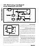
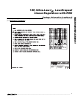
Detailed Description
The MAX8880/MAX8881 are low-dropout, low-quies-
cent current linear regulators designed primarily for
battery-powered applications (Figure 1). The MAX8880
provides an adjustable output voltage from 1.25V to 5V
using an external resistor-divider. The MAX8881 is
available in factory preset output voltages of 1.8V, 2.5V,
3.3V, and 5V. Both devices have a +1.25V reference,
error amplifier, MOSFET driver, and P-channel pass
transistor (Figure 2).
Low-Dropout Regulator
The 1.25V reference is connected to the error amplifi-
er’s inverting input. The error amplifier compares this
reference with the selected feedback voltage and
amplifies the difference. The MOSFET driver reads the
error signal and applies the appropriate drive to the P-
channel pass transistor. If the feedback voltage is lower
than the reference voltage, the pass-transistor gate is
pulled lower, allowing more current to pass, increasing
the output voltage. If the feedback voltage is higher
than the reference voltage, the pass-transistor gate is
driven higher, allowing less current to pass to the out-
put. The output voltage is fed back through either an
internal resistor voltage divider by externally connect-
ing FB to OUT (MAX8881), or an external resistor net-
work connected to FB (MAX8880). Additional blocks
include an output current limiter, reverse battery pro-
tection, a thermal sensor, shutdown logic, and a POK
comparator to indicate when the output is out of regula-
tion (Figure 2).
Internal P-Channel Pass Transistor
The MAX8880/MAX8881 feature a 2Ω P-channel MOS-
FET pass transistor. This provides advantages over
similar designs using PNP pass transistors, including
longer battery life. The P-channel MOSFET requires no
base drive, which reduces quiescent current consider-
ably. PNP-based regulators waste considerable current
in dropout when the pass transistor saturates. They
also use high base-drive currents under large loads.
The MAX8880/MAX8881 do not suffer from these prob-
lems and consume only 3.5µA of supply current (see
Typical Operating Characteristics).
Dropout Voltage
A regulator’s minimum input-output differential (or
dropout voltage) determines the lowest usable supply
voltage. In battery-powered systems, this determines
the useful end-of-life battery voltage. Because the
MAX8880/MAX8881 use a P-channel MOSFET pass
transistor, their dropout voltage is R
DS(ON)
(2Ω) multi-
plied by the load current (see Electrical Characteristics).
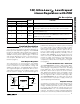
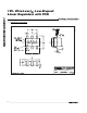
IN
R2*
100k
OUT
FB
GND
C2
4.7μF
C1
1μF
SHDN
2.5V TO 12V
REGULATION OK
POK
MAX8881
V
IN
VOUT
*OPTIONAL
Figure 1. Standard Application Circuit
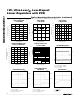
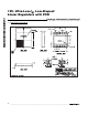
PIN
MAX888_ (SOT)
MAX888_ (TDFN)
NAME FUNCTION
1
4
IN Input Voltage. Bypass with a 1µF capacitor to GND.
2
2
GND Ground
3 3 OUT
Output Voltage. Bypass with a 4.7µF capacitor (<0.5Ω ESR) to GND for load
currents up to 200mA. For load currents up to 40mA, 1µF is acceptable.
41FB
Feedback Set Point, 1.25V (MAX8880 only). Output sense, connect to OUT
externally (MAX8881 only).
5 5 SHDN
ON/OFF Control. Regulator is ON when V
SHDN
> 2V. If unused, connect to
IN. If reverse battery protection of the SHDN input is desired, connect a
100kΩ resistor in series with SHDN.
6 6 POK
POK Output, Open Drain. Low when OUT is out of regulation or in shutdown.
Connect POK to OUT through a high-value resistor for a simple error
—
—
EP Exposed paddle (TDFN only). Connect to the circuit ground plane.
Pin Description