
Datasheet


(V
CC
= 5V, V
CM
= 0V, SHDN = LE = V
CC
(MAX9141 only), C
L
= 15pF, T
A
= T
MIN
to T
MAX
, unless otherwise noted. Typical values are
at T
A
= +25°C.) (Note 1)
Note 1: All devices are 100% production tested at T
A
= +25°C. Specifications over temperature are guaranteed by design.
Note 2: Inferred from PSRR test.
Note 3: Inferred from CMRR test. Note also that either or both inputs can be driven to the absolute maximum limit (0.3V beyond
either supply rail) without damage or false output inversion.
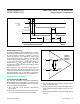
Note 4: V
OS
is defined as the center of the input-referred hysteresis zone. See Figure 1.
Note 5: The input-referred trip points are the extremities of the differential input voltage required to make the comparator output
change state. The difference between the upper and lower trip points is equal to the width of the input-referred hysteresis
zone. See Figure 1.
Note 6: The polarity of I
B
reverses direction as V
CM
approaches either supply rail.
Note 7: Specified over the full common-mode voltage range (V
CMR
).
Note 8: Specification is for current flowing into or out of the output pin for V
OUT
driven to any voltage from V
CC
to GND while the part
is in shutdown.
Note 9: Specified between any two channels in the MAX9142/MAX9144.
Note 10: Specified as the difference between t
PD+
and t
PD-
for any one comparator.
Note 11: Applies to the MAX9141 only for both SHDN and LE.
Note 12: Applies to the MAX9141 only. Comparator is active with LE driven high and is latched with LE driven low (V
OD
= 10mV). See
Figure 2.
Note 13: Applicable to the MAX9141 only. Comparator is active with the SHDN driven high and is shutdown with SHDN driven low.
Shutdown enable time is the delay when the SHDN is driven high to the time the output is valid. Shutdown disable time is the
delay when the SHDN is driven low to the time the comparator shuts down.
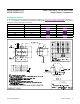
PARAMETER SYMBOL CONDITIONS MIN TYP MAX UNITS
Supply Current (Per Comparator) I
CC
V
CM
= V
CC
= 3V
MAX9141 165 275
µA
MAX9140,
T
A
= -40ºC to 85ºC
150 250
MAX9140AA_ _ 360
MAX9142/MAX9144 150 250
V
CM
= V
CC
= 5V
MAX9141 200 320
MAX9140,
T
A
= -40ºC to 85ºC
165 300
MAX9140AA_ _ 400
MAX9142/MAX9144 165 300
MAX9141 only, SHDN = GND;
V
CC
= V
CM
= 3V
12 30
Propagation Delay
t
PD+
,
t
PD-
V
CC
= 3V, V
OD
= 10mV 40 ns
Differential Propagation Delay dt
PD
V
OD
= 10mV (Note 9) 2 ns
Propagation Delay Skew V
OD
= 10mV (Note 10) 2 ns
Logic Input-Voltage High V
IH
(Note 11)
(V
CC
/2)
+0.4
V
CC
/2 V
Logic Input-Voltage Low V
IL
(Note 11) V
CC
/2
(V
CC
/2)
-0.4
V
Logic Input Current I
IL
, I
IH
V
LOGIC
= 0 to V
CC
(Note 11) 2 10 µA
Data-to-Latch Setup Time t
S
(Note 12) 16 ns
Latch-to-Data Hold Time t
H
(Note 12) 16 ns
Latch Pulse Width t
LPW
(Note 12) 45 ns
Latch Propagation Delay t
LPD
(Note 12) 60 ns
Shutdown Enable Time (Note 13) 1 µs
Shutdown Disable Time (Note 13) 5 µs
MAX9140/MAX9141/
MAX9142/MAX9144
40ns, Low-Power, 3V/5V, Rail-to-Rail
Single-Supply Comparators
www.maximintegrated.com
Maxim Integrated
│
3
Electrical Characteristics (continued)