
Datasheet


Detailed Description
The MAX9140/MAX9141/MAX9142/MAX9144 singlesup-
ply comparators feature internal hysteresis, high speed,
and low power. Their outputs are pulled to within 300mV
of either supply rail without external pullup or pulldown
circuitry. Rail-to-rail input voltage range and low-voltage
single-supply operation make these devices ideal for
portable equipment. The MAX9140/MAX9141/MAX9142/
MAX9144 interface directly to CMOS and TTL logic.
Most high-speed comparators oscillate in the linear region
because of noise or undesired parasitic feedback. This
tends to occur when the voltage on one input is at or equal
to the voltage on the other input. To counter the parasitic
effects and noise, the MAX9140/MAX9141/MAX9142/
MAX9144 have an internal hysteresis of 1.5mV.
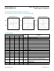
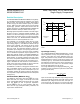
The hysteresis in a comparator creates two trip points:
one for the rising input voltage and one for the falling
input voltage (Figure 1). The difference between the trip
points is the hysteresis. The average of the trip points
is the offset voltage. When the comparator’s input volt-
ages are equal, the hysteresis effectively causes one
comparator input voltage to move quickly past the other,
thus taking the input out of the region where oscillation
occurs. Standard comparators require hysteresis to be
added with external resistors. The MAX9140/MAX9141/
MAX9142/MAX9144’s fixed internal hysteresis eliminates
these resistors. To increase hysteresis and noise margin
even more, add positive feedback with two resistors as a
voltage divider from the output to the noninverting input.
Figure 1 illustrates the case where IN- is fixed and IN+ is
varied. If the inputs were reversed, the figure would look
the same, except the output would be inverted.
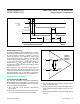
The MAX9141 includes an internal latch that allows stor-
age of comparison results. The LE pin has a high input
impedance. If LE is high, the latch is transparent (i.e., the
comparator operates as though the latch is not present).
The comparator’s output state is latched when LEis pulled
low (Figure 2).
Shutdown Mode (MAX9141 Only)
The MAX9141 shuts down when the SHDN pin is low.
When shut down, the supply current drops to less than
12μA, and the three-state output becomes high imped-
ance. The SHDN pin has a high-input impedance.
Connect SHDN to V
CC
for normal operation. Exit shut-
down with LE high (transparent state); otherwise, the
output will be indeterminate.
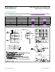
Input Stage Circuitry
The MAX9140/MAX9141/MAX9142/MAX9144 include
internal protection circuitry that prevents damage to the
precision input stage from large differential input volt-
ages. This protection circuitry consists of two back-toback
diodes between IN+ and IN- as well as two series 4.1kΩ
resistors (Figure 3). The diodes limit the differential volt-
age applied to the internal circuitry of the comparators to
be no more than 2V
F
, where V
F
is the forward voltage
drop of the diode (about 0.7V at +25°C).
For a large differential input voltage (exceeding 2V
F
), this
protection circuitry increases the input bias current at IN+
(source) and IN- (sink).
F
(IN+ - IN-) - 2V
Input Current
2 4.1k
=
×Ω
Input current with large differential input voltages should
not be confused with input bias current (I
B
). As long as the
differential input voltage is less than 2V
F
, this input cur-
rent is equal to I
B
. The output is in the correct logic state
if one or both inputs are within the common-mode range.
Figure 1. Input and Output Waveform, Noninverting Input
Varied
V
TRIP+
V
HYST
V
TRIP-
COMPARATOR
OUTPUT
V
OH
V
OL
V
TRIP+
+ V
TRIP-
2
V
OS
=
V
IN-
= 0
V
IN+
MAX9140/MAX9141/
MAX9142/MAX9144
40ns, Low-Power, 3V/5V, Rail-to-Rail
Single-Supply Comparators
www.maximintegrated.com
Maxim Integrated
│
7