
Datasheet


MAX9691/MAX9692/MAX9693
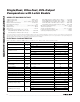
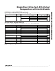
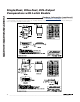
The timing diagram (Figure 3) illustrates the series of
events that complete the compare function, under
worst-case conditions. The top line of the diagram illus-
trates two latch-enable pulses. Each pulse is high for
the compare function and low for the latch function. The
first pulse demonstrates the compare function; part of
the input action takes place during the compare mode.
The second pulse demonstrates a compare function
interval during which there is no change in the input.
The leading edge of the input signal (illustrated as a
large-amplitude, small-overdrive pulse) switches the
comparator after time interval t
pd
. Output Q and Q tran-
sistors are similar in timing. The input signal must occur
at time t
s
before the latch falling edge, and must be
maintained for time t
h
after the edge to be acquired.
After t
h
, the output is no longer affected by the input sta-
tus until the latch is again strobed. A minimum latch
pulse width of t
pw(LE)
is needed for the strobe opera-
tion, and the output transitions occur after a time t
LE(±)
.
The MAX9691/MAX9692/MAX9693 will not false trip
(i.e., output invert) if one of the inputs is in the valid
common-mode range while the other input is outside
the common-mode range.
LATCH
ENABLE
DIFFERENTIAL
INPUT
VOLTAGE
Q
Q
LATCH
COMPARE
t
s
t
h
V
OD
V
IN
t
LE(+)
V
OS
50%
50%
50%
t
pw(LE)
t
pd
Figure 3. Timing Diagram
Single/Dual, Ultra-Fast, ECL-Output
Comparators with Latch Enable
_______________________________________________________________________________________ 7