
Datasheet


MAX9691/MAX9692/MAX9693
Single/Dual, Ultra-Fast, ECL-Output
Comparators with Latch Enable
8 _______________________________________________________________________________________
Definition of Terms
V
OS
Input Offset Voltage. The voltage required
between the input terminals to obtain 0V dif-
ferential at the output.
V
IN
Input Voltage Pulse Amplitude
V
OD
Input Voltage Overdrive
t
pd+
Input to Output High Delay. The propagation
delay measured from the time the input signal
crosses the input offset voltage to the 50%
point of an output low-to-high transition.
t
pd-
Input to Output Low Delay. The propagation
delay measured from the time the input signal
crosses the input offset voltage to the 50%
point of an output high-to-low transition.
t
LE(+)
Latch-Enable to Output High Delay. The prop-
agation delay measured from the 50% point of
the latch-enable signal low-to-high transition
to the 50% point of an output low-to-high tran-
sition.
t
LE(-)
Latch-Enable to Output Low Delay. The prop-
agation delay measured from the 50% point of
the latch-enable signal low-to-high transition
to the 50% point of an output high-to-low tran-
sition.
t
pw
(LE)
Latch-Enable Pulse Width. The minimum time
the latch-enable signal must be high to acquire
and hold an input signal.
t
s
Setup Time. The minimum time before the
negative transition of the latch-enable pulse
that an input signal must be present to be ac-
quired and held at the outputs.
t
h
Hold Time. The minimum time after the nega-
tive transition of the latch-enable signal that
an input signal must remain unchanged to be
acquired and held at the output.
∆
pd
Propagation Delay Skew. The difference in
propagation delay between the Q and Q out-
puts crossing each other in both directions.
P
DSP
Propagation Delay Dispersion. The change in
propagation delay as a result of the overdrive
of the input signal varying.
t
pdm
Propagation Delay Match (MAX9693 only).
The difference in propagation delay between
two separate channels.
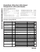
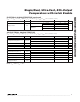
PART
TEMP
RANGE
PIN-PACKAGE
MAX9692EUB -40°C to +85°C 10 µMAX
MAX9692ESE -40°C to +85°C 16 Narrow SO
MAX9692EPE -40°C to +85°C 16 PDIP
MAX9693ESE -40°C to +85°C 16 Narrow SO
MAX9693EEE -40°C to +85°C 16 QSOP
MAX9693EPE -40°C to +85°C 16 PDIP
Ordering Information (continued)Chip Information
PROCESS: BiCMOS
Note: Devices are also available in lead(Pb)-free/RoHS-compli-
ant packages. Specify lead-free by adding a “+” after the part
number.