
Datasheet

MX7534/MX7535
Microprocessor-Compatible,
14-Bit DACs
10 ______________________________________________________________________________________
Compensation
A compensation capacitor, C1, may be needed when
the DAC is used with a high-speed output amplifier.
The capacitor cancels the pole formed by the DAC’s
output capacitance and internal feedback resistance.
Its value depends on the type of op amp used, but typi-
cal values range from 10pF to 33pF. Too small a value
causes output ringing, while excess capacitance over-
damps the output. Minimize C1’s size and improve out-
put settling performance by keeping the PC board
trace as short as possible and stray capacitance at
I
OUT
as small as possible.
Bypassing
Place a 1µF bypass capacitor, in parallel with a 0.01µF
ceramic capacitor, as close to the DAC’s V
DD
and GND
pins as possible. Use a 1µF tantalum bypass capacitor
to optimize high-frequency noise rejection. Place a
4.7µF decoupling capacitor at V
SS
to minimize the DAC
output leakage current.
The MX7534/MX7535 have high-impedance digital
inputs. To minimize noise pickup, connect them to
either V
DD
or GND terminals when not in use. Connect
active inputs to V
DD
or GND through high-value resis-
tors (1MΩ) to prevent static charge accumulation if
these pins are left floating, as might be the case when
a circuit card is left unconnected.
Op-Amp Selection
Input offset voltage (V
OS
), input bias current (I
B
), and
offset voltage drift (TC V
OS
) are three key parameters in
determining the choice of a suitable amplifier. To main-
tain specified accuracy with V
REF
of 10V, V
OS
should
be less than 30µV and I
B
should be less than 2nA.
Open-loop gain should be greater than 340,000.
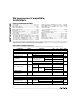
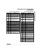
Maxim’s MAX400 has low V
OS
(10µV max), low I
B
(2nA), and low TC V
OS
(0.3µV/°C max). This op amp
can be used without requiring any adjustments. For
OP AMP
INPUT OFFSET
VOLTAGE (V
OS
)
INPUT BIAS
CURRENT (I
B
)
OFFSET VOLTAGE
DRIFT (TC V
OS
)
SETTLING
TO 0.003% FS
MAX400 10µV 2nA 0.3µV/°C 50µs
Maxim OP07 25µV 2nA 0.6µV/°C 50µs
AD554L* 500µV 25pA 5µV/°C 5µs
HA2620* 4mV 35nA 20µV/°C 0.8µs
Table 5. Amplifier Performance Comparisons
* AD544L is an Analog Devices part; HA2620 is a Harris Semiconductor part.
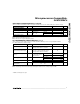
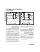
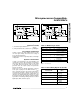
R4
33Ω
R3
100Ω
INPUT
DATA
SIGNAL
GROUND
A1
A2
7–14
620
5
4
3
2
191
C1
33pF
V
DD
V
DD
R
L
V
SS
MX7534
REF RFB
IOUT
AGNDS
AGNDF
DGNDD7–D0
+
+
V
IN
NOTE: CONTROL INPUTS OMITTED FOR CLARITY.
V
O
Figure 6a. Unipolar Binary Operation with Forced Ground
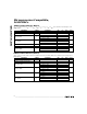
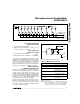
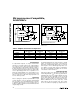
R2
10Ω
R1
20Ω
INPUT
DATA
SIGNAL
GROUND
ANALOG
GROUND
A1
A2
8–21
7
27
6
5
4
32621
C1
33pF
V
DD
V
DD
R
L
V
SS
MX7535
REFF REFS RFB
IOUT
AGNDS
AGNDF
DGNDD13–D0
+
+
VOLTAGE
REFERENCE
NOTE: CONTROL INPUTS OMITTED FOR CLARITY.
V
O
Figure 6b. Unipolar Binary Operation with Forced Ground for
Remote Load