
Datasheet


medium-frequency applications, the OP27 is recom-
mended. For higher-frequency applications, the HA-
2620 is recommended. However, these op amps
require external offset adjustment (Table 5).
________Microprocessor Interfacing
8086 with MX7535
The MX7534/MX7535 interface to both 8-bit and 16-bit
processors. Figure 9a shows the 8086 16-bit processor
interfacing to a single MX7535. In this setup, the double-
buffering feature of the DAC is not used. AD0–AD13 of
the 16-bit data bus are connected to the DAC data bus
(D0–D13). The 14-bit word is written to the DAC in one
MOV instruction, and the analog output responds imme-
diately. In this example, the DAC address is D000. Table
6a shows a software routine for Figure 9a.
In a multiple DAC system, the double buffering of the
DAC chips allows the user to simultaneously update all
DACs. In Figure 10, a 14-bit word is loaded to each of
the DAC’s input registers in sequence. Then, with one
instruction to the appropriate address, CS4 (i.e., LDAC)
is brought low, updating all the DACs simultaneously.
8086 with MX7534
Figure 9b shows an interface circuit to a 16-bit micro-
processor. The bottom 8 bits (AD0–AD7) of the 16-bit
data bus are connected to the DAC data bus. The
14-bit word is loaded in two bytes, using the MOV
instruction. A further MOV loads the DAC register and
causes the analog data to appear at the converter out-
put. For the example given here, the appropriate DAC
register addresses are D002, D004, and D006. Table
6b shows the program for loading the DAC.
8085A with MX7534
A typical interface circuit is shown in Figure 9c. The
DAC is treated as four memory locations addressed by
A0 and A1. In standard operation, three of these memo-
ry locations are used. Table 6c shows a sample pro-
gram for loading the DAC with a 14-bit word. The
MX7534 has address locations 3000–3003.
The six MSBs are written into location 3001, and eight
LSBs are written to 3002. Then, with a write instruction to
3003, the full 14-bit word is loaded to the DAC register.
MX7534/MX7535
Microprocessor-Compatible,
14-Bit DACs
______________________________________________________________________________________ 11
R
L
INPUT
DATA
A3
8–21
7
27
6
5
4
3
2
261
C1
33pF
V
DD
V
0
V
SS
V
DD
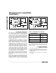
MX7535
REFF REFS RFB
IOUT
AGNDS
AGNDF
DGNDD13–D0
+
A2
+
A1
+
NOTE: CONTROL INPUTS OMITTED FOR CLARITY.
Figure 7. Driving the MX7535 with a Remote Voltage Reference
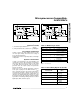
AGND
DGND
REF
PIN 1 AD544*
OUTPUT
V
SS
V
DD
C1 LOCATION
V+
V-
NOTE:
LAYOUT IS FOR DOUBLE-SIDED
PCB. BOLD LINE INDICATES
TRACK ON COMPONENT SIDE.
*AD544 IS AN ANALOG DEVICES PART.
PIN 1 MX7534
Figure 8. Suggested Layout for MX7534 Incorporating Output
Amplifier