
Datasheet


MX7534/MX7535
Microprocessor-Compatible,
14-Bit DACs
12 ______________________________________________________________________________________
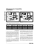
MC68000 with MX7535
Figure 11a shows an interface diagram. The following
routine writes data to the DAC input registers and then
outputs the data via the DAC register:
01000 MOVE.W #W,D0 DAC data, W, loaded
into Data Register 0.
MOVE.W D0,$E000 Data W transferred
between D0 and DAC
Register.
MOVE.B #228,D7 Control returned to the
System.
TRAP #14 Monitor Program
MC68000 with MX7534
Figure 11b shows the MC68000 interface diagram. The
following routine writes data to the DAC input registers
and then outputs the data via the DAC register:
.A2 E003 Address Register 2
loaded with E003.
01000 MOVE.W #W,D0 DAC data, W, loaded
into Data Register 0.
MOVEP.W D0,$0000
(A2)
Data W transferred
between D0 and the
DAC’s Input Register.
High-ordered byte trans-
ferred first. Memory
address specified using
the address register
indirect plus displace-
ment addressing mode.
Address used here
(E003) is odd, so data is
transferred on the low-
order half of the data
bus (D0–D7).
MOVE.W D0,$E006 This instruction provides
appropriate signals to
transfer data W from
the DAC Input Register
to the DAC Register,
which controls the R-2R
ladder switches.
MOVE.B #228,D7 Control returned to the
System.
TRAP #14 Monitor Program
Since this interfacing system uses only the lower half of
the data bus, it is also suitable for use with the
MC68008, which provides the user with an 8-bit data
bus instead of the MC68000’s 16-bit bus.
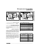
ADDRESS
DECODE
LATCH
ADDRESS BUS
CS
WR
D0–D7
A1 A0
MX7534*
*SOME CIRCUITRY OMITTED FOR CLARITY
AE
A8–A15
8085A
DATA BUS
AD0–AD7
WR
Figure 9c. MX7534—8085A Interface Circuit
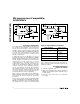
ADDRESS
DECODE
16-BIT
LATCH
ADDRESS BUS
DATA BUS
ALE
8086
CS
WR
D0–D7
A2
A1 A0
A1
MX7534*
*SOME CIRCUITRY OMITTED FOR CLARITY
ADDRESS BUS
AD0–AD15
WR
Figure 9b. MX7534—8086 Interface Circuit
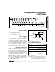
ADDRESS
DECODE
16-BIT
LATCH
ADDRESS BUS
DATA BUS
ALE
8086
LDAC
CSLSB
CSMSB
WR
D0–D13
AD13
AD0
MX7535*
*SOME CIRCUITRY OMITTED FOR CLARITY
AD0–AD15
WR
Figure 9a. MX7535—8086 Interface Circuit