
Datasheet

MX7534/MX7535
Microprocessor-Compatible,
14-Bit DACs
_______________________________________________________________________________________ 7
Zero-Offset Adjustment
(Figures 4a and 4b)
1) Load the DAC register with all 0s.
2) Adjust the offset of amplifier A1 so that V
0
(see fig-
ure) is at a minimum (i.e., ≤ 30µV).
Gain Adjustment
(Figures 4a and 4b)
1) Load the DAC register with all 1s.
2) Trim potentiometer R1 so that V
OUT
= -V
IN
(
16383
)
16384
In fixed-reference applications, adjust full scale by
omitting R1 and R2 and trimming the reference voltage
magnitude. In many applications, the excellent Gain
Tempco and Gain Error specifications eliminate the
need for gain adjustment. However, if trims are
required and the DAC is to operate over a wide temper-
ature range, use low-tempco (>300ppm/°C) resistors.
Bipolar Operation
(4-Quadrant Multiplication)
Bipolar or 4-quadrant operation is shown in Figures 5a
and 5b. This configuration provides for offset binary
coding. Table 4 shows DAC codes and the corre-
sponding analog outputs for Figures 5a and 5b. With
the DAC loaded to 10 0000 0000 0000, either adjust R1
for V
OUT
= 0V, or omit R1 and R2 and adjust the ratio of
R5 and R6 for V
OUT
= 0V. Adjust the amplitude of V
IN
or vary the value of R7 for full-scale trimming.
Resistors R5, R6, and R7 must be matched to 0.003%.
Mismatch of R5 and R6 causes both offset and full-
scale errors. For wide temperature range operation,
use resistors of the same material so that their tempera-
ture coefficients match and track.
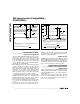
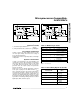
2R 2R
G F E D C B A S10 S9 S0
2R 2R 2R 2R 2R 2R 2R
R
RR
2R2R
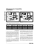
R/4
RFB
IOUT
AGNDS
AGNDF
*NOTE: VALID FOR MX7535. IN MX7534, 0REFS AND 0REFF ARE REPLACED BY ONE PIN: REF.
REFS*
REFF*
R/4
+
–
AGNDS
AGNDF
IOUT
RFB
I
LEAKAGE
g(V
REF
, N) C
OUT
R
O
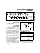
Figure 2. Simplified Circuit Diagram
Figure 3. Equivalent Analog Output Circuit
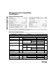
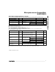
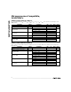
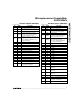
Table 1. MX7534 Logic States
A1 A2 FUNCTION
X 1 X X Device not selected (Note 1)
1 X X X No data transfer
0000
DAC loaded directly from
Data Bus (Note 2)
0001
MS Input Register loaded
from Data Bus
0010
LS Input Register loaded
from Data Bus
0011
DAC Register loaded from
Input Registers
Note 1: X = Don’t Care.
Note 2: When A1 = 0 and A0 = 0, all DAC registers are trans-
parent. By placing all 0s or all 1s on the data inputs, the
user can load the DAC to zero or full-scale output in
one write operation. This simplifies system calibration.