
Datasheet

MX7534/MX7535
Grounding Considerations
Since IOUT and the output amplifier noninverting input
are sensitive to offset voltages, connect nodes that
must be grounded directly to a single-point ground
through a separate, very-low-resistance path. Note that
the output currents at IOUT and AGNDF vary with input
code and create code-dependent error if these termi-
nals are connected to ground (or a virtual ground)
through a resistive path.
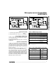
To obtain high accuracy, it is important to use a proper
grounding technique. The two AGND pins (AGNDF‚
AGNDS) provide flexibility in this respect. In Figures 4a
and 4b, AGNDS and AGNDF are shorted together
externally and an extra op amp, A2, is not used.
Voltage-drops due to bond-wire resistance are not
compensated for in this circuit; this could create a lin-
earity error of approximately 0.1LSB due to bond-wire
resistance alone. This can be eliminated by using the
circuits shown in Figures 6a and 6b, where A2 main-
tains AGNDS at signal ground potential. By using
force/sense techniques, all switch contacts on the DAC
are kept at exactly the same potential, and any error
caused by bond-wire resistance is eliminated.
Figure 7 shows a remote voltage reference driving the
MX7535. Op amps A2 and A3 compensate for voltage
drops along the reference input line and analog
ground line.
Figure 8 shows a printed circuit board (PCB) layout with
a single output amplifier for the MX7534. The input to
REF (Pin 1) is shielded to reduce AC feedthrough, while
the digital inputs are shielded to minimize digital
feedthrough. The traces connecting IOUT and AGNDS
to the inverting and noninverting op amp inputs are
kept as short as possible. Gain trim components, R3
and R4, are omitted.
Zero-Offset Adjustment
(Figures 6a and 6b)
1) Load DAC register with all 0s.
2) Adjust offset of amplifier A2 for minimum potential at
AGNDS. This potential should be ≤30µV with respect
to signal ground.
3) Adjust A1’s offset so that V
OUT
is at a minimum
(i.e., ≤30µV).
Microprocessor-Compatible,
14-Bit DACs
8 _______________________________________________________________________________________
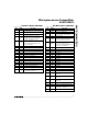
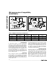
Table 2. Unipolar Binary Code Table
BINARY NUMBER IN
DAC REGISTER
ANALOG OUTPUT
(V
OUT)
MSB LSB
11 1111 1111 1111
10 0000 0000 0000
00 0000 0000 0001
00 0000 0000 0000
-V
IN
(
16383
)
16384
-V
IN
(
8192
)
= -
1
V
IN
16384 2
-V
IN
(
1
)
16384
0V
R1
100Ω
R2
33Ω
INPUT
DATA
ANALOG
GROUND
A0
A1
A1
7–14
CS
WR
16
620
5
4
3
2191
C1
33pF
V
DD
V
IN
V
SS
MX7534
REF RFB
IOUT
AGNDS
AGNDF
DGND
D7–D0
15
18
17
V
O
R1
20Ω
R2
10Ω
INPUT
DATA
ANALOG
GROUND
LDAC
A1
CSMSB
8–21
CSLSB
WR
23
727
6
5
4
32261
C1
33pF
V
DD
V
IN
V
SS
MX7535
REFF
REFS
RFB
IOUT
AGNDS
AGNDF
DGNDD13–DO
22
25
24
V
O
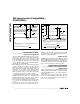
Figure 4a. Unipolar Binary Operation
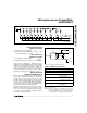
Figure 4b. Unipolar Binary Operation