
Datasheet

MX7534/MX7535
Microprocessor-Compatible,
14-Bit DACs
_______________________________________________________________________________________ 9
Gain Adjustment
(Figures 6a and 6b)
1) Load DAC register with all 1s.
2) Trim potentiometer R3 so that V
OUT
= -
(
16383
)
V
IN
16384
Low-Leakage Configuration
Leakage current in the DAC flowing into the I
OUT
line
can cause gain, linearity, and offset errors. Leakage is
worse at high temperatures.
Negatively bias V
SS
for a high-temperature, low-leakage
configuration.
Dynamic Considerations
In static or DC applications, the output amplifier’s AC
characteristics are not critical. In higher-speed applica-
tions, where either the reference input is an AC signal
or the DAC output must quickly settle to a new pro-
grammed value, the output op amp’s AC parameters
must be considered.
Another error source in dynamic applications is the par-
asitic signal coupling from the REF terminal to I
OUT
.
This is normally a function of board layout and lead-to-
lead package capacitance. Signals can also be inject-
ed into the DAC outputs when the digital inputs are
switched. This digital feedthrough depends on circuit-
board layout and on-chip capacitive coupling. Minimize
layout-induced feedthrough with guard traces between
digital inputs, REF, and DAC outputs.
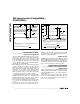
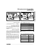
R1
100Ω
R2, 33Ω
R6
20k
R7
20k
R5 10k
R8, 5k,10%
INPUT
DATA
ANALOG
GROUND
A0
A1
A2
A1
7–14
WR
CS
16
620
5
4
3
2191
C1
33pF
V
IN
V
DD
V
SS
MX7534
REF RFB
IOUT
AGNDS
AGNDF
DGNDD7–D0
15
18
17
+
+
V
O
Figure 5a. Bipolar Operation
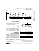
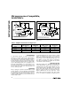
R1
20Ω
R2 10Ω
R6
20k
R7
20k
R5
10k
R8, 5k,10%
INPUT
DATA
ANALOG
GROUND
LDAC
A1
A2
CSMSB
8–21
WR
CSLSB
23
7
27
6
5
4
3
2
261
C1
33pF
V
IN
V
DD
V
SS
MX7535
REFF REFS RFB
IOUT
AGNDS
AGNDF
DGNDD13–D0
22
25
24
+
+
V
O
Figure 5b. Bipolar Operation
FUNCTION
0 1 1 0 Load MS Input Register
1 0 1 0 Load LS Input Register
0010
Load LS and MS Input
Registers
110X
Load DAC Register
from Input Register
0000
All registers are
transparent.
1 1 1 X No operation
X X 1 1 No operation
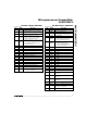
Table 3. MX7535 Logic States
Table 4. Offset Binary Bipolar Code Table
BINARY NUMBER IN
DAC REGISTER
Analog Output
(V
OUT)
MSB LSB
11 1111 1111 1111
10 0000 0000 0001
10 0000 0000 0000
01 1111 1111 1111
00 0000 0000 0000
+V
IN
(
8191
)
8192
+V
IN
(
1
)
8192
0
-V
IN
(
1
)
8192
-V
IN
(
8192
)
= -V
IN
8192
Note: X = Don’t Care.