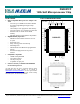
DS5001FP 128k Soft Microprocessor Chip www.maxim-ic.
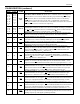
DS5001FP ORDERING INFORMATION PART TEMP RANGE DS5001FP-16 DS5001FP-16+ DS5001FP-16N DS5001FP-16N+ DS5001FP-12-44 DS5001FP-12-44+ 0°C to +70°C 0°C to +70°C -40°C to +85°C -40°C to +85°C 0°C to +70°C 0°C to +70°C MAX CLOCK SPEED (MHz) 16 16 16 16 12 12 PINPACKAGE 80 MQFP 80 MQFP 80 MQFP 80 MQFP 44MQFP 44 MQFP + Denotes a Pb-free/RoHS-compliant device.
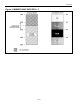
DS5001FP Figure 1.
DS5001FP PIN DESCRIPTION PIN 80 PIN 44 PIN 11, 9, 7, 31 5, 1, 79, (P0.5) 77, 75 15, 17, 19, 21, 44 25, 27, (P1.3) 29, 31 49, 50, 51, 56, — 58, 60, 64, 66 NAME FUNCTION P0.0– P0.7 General-Purpose I/O Port 0. This port is open-drain and cannot drive a logic 1. It requires external pullups. Port 0 is also the multiplexed expanded address/data bus. When used in this mode, it does not require pullups. P1.0– P1.7 General-Purpose I/O Port 1 P2.0– P2.7 General-Purpose I/O Port 2.
DS5001FP PIN DESCRIPTION (continued) PIN 80 PIN 44 PIN 53, 16, 41, 36, 8, 18, 42, 32, 80, 76, 30, 34, 4, 6, 20, 35, 43, 24, 26, 1, 2, 3, 28, 30, 4, 5, 7, 33, 35, 9 37 71, 69, 28, 26, 67, 65, 24, 23, 61, 59, 21, 20, 57, 55 19, 18 NAME FUNCTION BA14– BA0 Byte-Wide Address Bus Bits 14–0. This bus is combined with the nonmultiplexed data bus (BD7–0) to access NV SRAM. Decoding is performed using CE1 through CE4 . Therefore, BA15 is not actually needed. Read/write access is controlled by R/ W .
DS5001FP PIN DESCRIPTION (continued) PIN 80 PIN 44 PIN NAME 42 — VRST 43 — PF 14 40 MSEL 73 — N.C. FUNCTION This I/O pin (open drain with internal pullup) indicates that the power supply (VCC) has fallen below the VCCmin level and the micro is in a reset state. When this occurs, the DS5001FP drives this pin to a logic 0. Because the micro is lithiumbacked, this signal is guaranteed even when VCC = 0V. Because it is an I/O pin, it also forces a reset if pulled low externally.
DS5001FP Figure 2.
DS5001FP Figure 3. MEMORY MAP IN PARTITIONABLE MODE (PM = 0) NOTE: PARTITIONABLE MODE IS NOT SUPPORTED WHEN MSEL PIN = 0 (128kB MODE).
DS5001FP Figure 4.
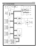
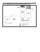
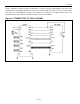
DS5001FP Figure 5 illustrates a typical memory connection for a system using a 128kB SRAM. Note that in this configuration, both program and data are stored in a common RAM chip Figure 6 shows a similar system with using two 32kB SRAMs. The byte-wide address bus connects to the SRAM address lines. The bidirectional byte-wide data bus connects the data I/O lines of the SRAM. Figure 5.
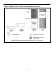
DS5001FP Figure 6. DS5001FP CONNECTION TO 64k x 8 SRAM POWER MANAGEMENT The DS5001FP monitors VCC to provide power-fail reset, early warning power-fail interrupt, and switch over to lithium backup. It uses an internal bandgap reference in determining the switch points. These are called VPFW, VCCMIN, and VLI, respectively. When VCC drops below VPFW, the DS5001FP performs an interrupt vector to location 2Bh if the power-fail warning was enabled. Full processor operation continues regardless.
DS5001FP ABSOLUTE MAXIMUM RATINGS Voltage Range on Any Pin Relative to Ground…………………………..…………………….-0.3V to (VCC + 0.5V) Voltage Range on VCC Related to Ground………………………………………………………………-0.3V to 6.0V Operating Temperature Range………………………………………………………………………...-40°C to +85°C Storage Temperature Range (Note 1)………………………………………………………………..-55°C to +125°C Soldering Temperature…………………………………………………….
DS5001FP DC CHARACTERISTICS (continued) (VCC = 5V ±10%, TA = 0°C to +70°C.) PARAMETER Input Leakage Current 0.
DS5001FP AC CHARACTERISTICS: EXPANDED BUS MODE TIMING SPECIFICATIONS (VCC = 5V ±10%, TA = 0°C to +70°C.
DS5001FP EXPANDED PROGRAM-MEMORY READ CYCLE EXPANDED DATA-MEMORY READ CYCLE 15 of 27
DS5001FP EXPANDED DATA-MEMORY WRITE CYCLE 16 of 27
DS5001FP AC CHARACTERISTICS: EXTERNAL CLOCK DRIVE (VCC = 5V ±10%, TA = 0°C to +70°C.
DS5001FP AC CHARACTERISTICS: POWER CYCLE TIME (VCC = 5V ±10%, TA = 0°C to +70°C.
DS5001FP AC CHARACTERISTICS: SERIAL PORT TIMING—MODE 0 (VCC = 5V ±10%, TA = 0°C to +70°C.
DS5001FP AC CHARACTERISTICS: BYTE-WIDE ADDRESS/DATA BUS TIMING (VCC = 5V ±10%, TA = 0°C to +70°C.
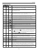
DS5001FP BYTE-WIDE BUS TIMING RPC AC CHARACTERISTICS: DBB READ (VCC = 5V ±10%, TA = 0°C to +70°C.) # 54 55 56 57 58 59 PARAMETER CS , A0 Setup to RD CS , A0 Hold After RD RD Pulse Width CS , A0 to Data-Out Delay RD to Data-Out Delay RD to Data-Float Delay SYMBOL tAR tRA tRR tAD tRD tRDZ MIN 0 0 160 0 MAX 130 130 85 UNITS ns ns ns ns ns ns RPC AC CHARACTERISTICS: DBB WRITE (VCC = 5V ±10%, TA = 0°C to +70°C.
DS5001FP AC CHARACTERISTICS: DMA (VCC = 5V ±10%, TA = 0°C to +70°C.) # 65 66 PARAMETER DACK to WR or RD RD or WR to DACK 67 68 DACK to Data Valid SYMBOL tACC tCAC MIN 0 0 MAX UNITS ns ns tACD tCRQ 0 130 110 ns ns SYMBOL tPRA tPRI MIN 48 48 MAX UNITS CLKS CLKS RD or WR to DRQ Cleared AC CHARACTERISTICS: PROG (VCC = 5V ±10%, TA = 0°C to +70°C.
DS5001FP RPC TIMING MODE 23 of 27
DS5001FP NOTES: All parameters apply to both commercial and industrial temperature operation unless otherwise noted. 1) All voltages are referenced to ground. 2) Maximum operating ICC is measured with all output pins disconnected; XTAL1 driven with tCLKR, tCLKF = 10ns, VIL = 0.5V; XTAL2 disconnected; RST = PORT0 = VCC, MSEL = VSS. 3) Idle mode, IIDLE, is measured with all output pins disconnected; XTAL1 driven with tCLKR, tCLKF = 10ns, VIL = 0.5V; XTAL2 disconnected; PORT0 = VCC, RST = MSEL = VSS.
DS5001FP PACKAGE INFORMATION (The package drawing(s) in this data sheet may not reflect the most current specifications. For the latest package outline information, go to www.maxim-ic.com/DallasPackInfo.) 80-PIN MQFP DIM A A1 A2 B C D D1 E E1 e L MM MIN MAX 3.40 0.25 2.55 2.87 0.30 0.50 0.13 0.23 23.70 24.10 19.90 20.10 17.70 18.10 13.90 14.10 0.80 BSC 0.65 0.
DS5001FP 44-PIN MQFP 26 of 27
DS5001FP REVISION HISTORY The following represent the key differences between the 112795 and 073096 version of the DS5001FP data sheet. Please review this summary carefully. 1) Change VCC02 specification from VLI - 0.5 to VLI - 0.65 (PCN F62501). 2) Update mechanical specifications. The following represent the key differences between the 073096 and 111996 version of the DS5001FP data sheet. Please review this summary carefully. 1) Change VCC01 from VCC - 0.3 to VCC - 0.35.