
Datasheet


MAX4238/MAX4239
Ultra-Low Offset/Drift, Low-Noise,
Precision SOT23 Amplifiers
4 _______________________________________________________________________________________
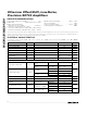
ELECTRICAL CHARACTERISTICS
(2.7V ≤ V
CC
≤ 5.5V, V
CM
= GND = 0V, V
OUT
= V
CC
/2, R
L
= 10kΩ connected to V
CC
/2, SHDN = V
CC
, T
A
= -40
°
C to +125
°
C, unless other-
wise noted.) (Note 5)
PARAMETER SYMBOL CONDITIONS MIN TYP MAX UNITS
T
A
= -40°C to +85°C 2.5
Input Offset Voltage V
OS
(Note 1)
T
A
= -40°C to +125°C 3.5
µV
Input Offset Drift TCV
OS
(Note 1) 10 nV/°C
Common-Mode Input Voltage
Range
V
CM
Inferred from CMRR test
GND -
0.05
V
CC
-
1.4
V
T
A
= -40°C to +85°C 115
Common-Mode Rejection Ratio CMRR
GN D - 0.05V ≤
V
C M
≤ V
C C
-
1.4V ( N ote 1)
T
A
= -40°C to +125°C90
dB
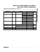
Power-Supply Rejection Ratio PSRR 2.7V ≤ V
CC
≤ 5.5V (Note 1) 120 dB
T
A
= -40°C to +85°C 125
R
L
= 10kΩ,
0.1V ≤ V
OUT
≤ V
CC
- 0.1V
(Note 1)
T
A
= -40°C to +125°C95
dB
0.1V ≤ V
OUT
≤ V
CC
- 0.1V,
T
A
= -40°C to +85°C
120
Large-Signal Voltage Gain A
VOL
R
L
= 1kΩ
(Note 1)
0.2V ≤ V
OUT
≤ V
CC
- 0.2V,
T
A
= -40°C to +125°C
80
dB
V
CC
- V
OH
20
R
L
= 10kΩ
V
OL
20
V
CC
- V
OH
100
Output Voltage Swing V
OH
/V
OL
R
L
= 1kΩ
V
OL
100
mV
Output Leakage Current
0V ≤ V
OUT
≤ V
CC
, SHDN = GND (Note
2µA
Supply Voltage Range V
CC
Inferred by PSRR test 2.7 5.5 V
SHDN = V
CC
, no load, V
CC
= 5.5V 900
Supply Current I
CC
SHDN = GND, V
CC
= 5.5V 2
µA
Shutdown Logic High V
IH
2.2 V
Shutdown Logic Low V
IL
0.7 V
Shutdown Input Current 0V ≤ V
SHDN
≤ V
CC
2µA
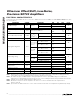
Note 1: Guaranteed by design. Thermocouple and leakage effects preclude measurement of this parameter during production
testing. Devices are screened during production testing to eliminate defective units.
Note 2: IN+ and IN- are gates to CMOS transistors with typical input bias current of 1pA. CMOS leakage is so small that it is
impractical to test and guarantee in production. Devices are screened during production testing to eliminate defective units.
Note 3: Leakage does not include leakage through feedback resistors.
Note 4: Overload recovery time is the time required for the device to recover from saturation when the output has been
driven to either rail.
Note 5: Specifications are 100% tested at T
A
= +25
°
C, unless otherwise noted. Limits over temperature are guaranteed by design.