
Datasheet


Detailed Description
The MAX4238/MAX4239 are high-precision amplifiers
that have less than 2.5µV of input-referred offset and
low 1/f noise. These characteristics are achieved
through a patented autozeroing technique that samples
and cancels the input offset and noise of the amplifier.
The pseudorandom clock frequency varies from 10kHz
to 15kHz, reducing intermodulation distortion present in
chopper-stabilized amplifiers.
Offset Error Sources
To achieve very low offset, several sources of error
common to autozero-type amplifiers need to be consid-
ered. The first contributor is the settling of the sampling
capacitor. This type of error is independent of input-
source impedance, or the size of the external gain-set-
ting resistors. Maxim uses a patented design technique
to avoid large changes in the voltage on the sampling
capacitor to reduce settling time errors.
The second error contributor, which is present in both
autozero and chopper-type amplifiers, is the charge
injection from the switches. The charge injection
appears as current spikes at the input, and combined
with the impedance seen at the amplifier’s input, con-
tributes to input offset voltage. Minimize this
feedthrough by reducing the size of the gain-setting
resistors and the input-source impedance. A capacitor
in parallel with the feedback resistor reduces the
amount of clock feedthrough to the output by limiting
the closed-loop bandwidth of the device.
The design of the MAX4238/MAX4239 minimizes the
effects of settling and charge injection to allow specifi-
cation of an input offset voltage of 0.1µV (typ) and less
than 2.5µV over temperature (-40°C to +85°C).
1/f Noise
1/f noise, inherent in all semiconductor devices, is
inversely proportional to frequency. 1/f noise increases
3dB/octave and dominates amplifier noise at lower fre-
quencies. This noise appears as a constantly changing
voltage in series with any signal being measured. The
MAX4238/MAX4239 treat 1/f noise as a slow varying
offset error, inherently canceling the 1/f noise.
MAX4238/MAX4239
Ultra-Low Offset/Drift, Low-Noise,
Precision SOT23 Amplifiers
_______________________________________________________________________________________ 7
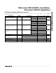
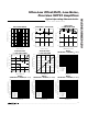
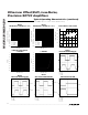
Typical Operating Characteristics (continued)
(V
CC
= 5V, V
CM
= 0V, R
L
= 10kΩ connected to V
CC
/2, SHDN = V
CC
, T
A
= +25°C, unless otherwise noted.)
SHUTDOWN WAVEFORM
MAX4238/39 toc20
R
L
= 10kΩ
C
L
= 100pF
10µs/div
OUT
2V/div
1V/div
SHDN
DC TO 10Hz NOISE
MAX4238/39 toc19
V
CC
= 2.5V
V
EE
= -2.5V
1s/div
OUT
2µV/div
PIN
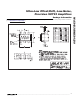
SOT23 SO
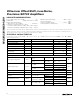
NAME FUNCTION
1 6 OUT Amplifier Output
2 4 GND Ground
3 3 IN+ Noninverting Input
4 2 IN- Inverting Input
51SHDN
Shutdown Input. Active low
shutdown, connect to V
CC
for
normal operation.
67V
CC
Positive Power Supply
— 5, 8 N.C.
No Connection. Not internally
connected.
Pin Description