
Datasheet

±15kV ESD-Protected, Slew-Rate-Limited,
Low-Power, RS-485/RS-422 Transceivers
Supply Voltage (V
CC
).............................................................12V
Control Input Voltage (
–
R
—
E
–
, DE)...................-0.5V to (V
CC
+ 0.5V)
Driver Input Voltage (DI).............................-0.5V to (V
CC
+ 0.5V)
Driver Output Voltage (Y, Z; A, B) ..........................-8V to +12.5V
Receiver Input Voltage (A, B).................................-8V to +12.5V
Receiver Output Voltage (RO)....................-0.5V to (V
CC
+ 0.5V)
Continuous Power Dissipation (T
A
= +70°C)
8-Pin Plastic DIP (derate 9.09mW/°C above +70°C) ....727mW
14-Pin Plastic DIP (derate 10.00mW/°C above +70°C) ..800mW
8-Pin SO (derate 5.88mW/°C above +70°C).................471mW
14-Pin SO (derate 8.33mW/°C above +70°C)...............667mW
Operating Temperature Ranges
MAX4_ _C_ _/MAX1487EC_ A .............................0°C to +70°C
MAX4_ _E_ _/MAX1487EE_ A...........................-40°C to +85°C
Storage Temperature Range .............................-65°C to +160°C
Lead Temperature (soldering, 10sec) .............................+300°C
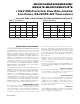
DC ELECTRICAL CHARACTERISTICS
(V
CC
= 5V ±5%, T
A
= T
MIN
to T
MAX
, unless otherwise noted.) (Notes 1, 2)
Stresses beyond those listed under “Absolute Maximum Ratings” may cause permanent damage to the device. These are stress ratings only, and functional
operation of the device at these or any other conditions beyond those indicated in the operational sections of the specifications is not implied. Exposure to
absolute maximum rating conditions for extended periods may affect device reliability.
ABSOLUTE MAXIMUM RATINGS
PARAMETER SYMBOL MIN TYP MAX UNITS
Driver Common-Mode Output
Voltage
V
OC
3 V
Change in Magnitude of Driver
Differential Output Voltage for
Complementary Output States
ΔV
OD
0.2 V
Change in Magnitude of Driver
Common-Mode Output Voltage
for Complementary Output States
ΔV
OD
0.2 V
Input High Voltage V
IH
2.0 V
Input Low Voltage V
IL
0.8 V
Input Current I
IN1
±2 µA
Differential Driver Output (no load) V
OD1
5 V
2
V
Differential Driver Output
(with load)
V
OD2
1.5 5
1.0
-0.8
mA
0.25
mA
-0.2
Receiver Differential Threshold
Voltage
-0.2 0.2 V
Receiver Input Hysteresis ΔV
TH
70 mV
Receiver Output High Voltage V
OH
3.5
Receiver Output Low Voltage V
OL
0.4
V
Three-State (high impedance)
Output Current at Receiver
I
OZR
±1 µA
12 kΩ
CONDITIONS
DE = 0V;
V
CC
= 0V or 5.25V,
all devices except
MAX487E/MAX1487E
R = 27Ω or 50Ω, Figure 8
R = 27Ω or 50Ω, Figure 8
R = 27Ω or 50Ω, Figure 8
DE, DI,
–
R
—
E
–
MAX487E/MAX1487E,
DE = 0V, V
CC
= 0V or 5.25V
DE, DI,
–
R
—
E
–
DE, DI,
–
R
—
E
–
-7V ≤ V
CM
≤ 12V
V
CM
= 0V
I
O
= -4mA, V
ID
= 200mV
I
O
= 4mA, V
ID
= -200mV
R = 50Ω (RS-422)
0.4V ≤ V
O
≤ 2.4V
R = 27Ω (RS-485), Figure 8
-7V ≤ V
CM
≤ 12V, all devices except
MAX487E/MAX1487E
Receiver Input Resistance R
IN
-7V ≤ V
CM
≤ 12V, MAX487E/MAX1487E 48 kΩ
V
TH
I
IN2
Input Current
(A, B)
V
IN
= 12V
V
IN
= -7V
V
IN
= 12V
V
IN
= -7V
V
MAX481E/MAX483E/MAX485E/
MAX487E–MAX491E/MAX1487E
2
Maxim Integrated