
Datasheet


Single/Dual/Quad, Ultra-High-Speed, +3V/+5V,
Beyond-the-Rails Comparators
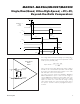
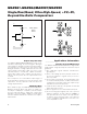
Output Stage Circuitry
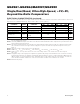
The MAX961–MAX964/MAX997/MAX999 contain a cur-
rent-driven output stage, as shown in Figure 4. During an
output transition, I
SOURCE
or I
SINK
is pushed or pulled to
the output pin. The output source or sink current is high
during the transition, creating a rapid slew rate. Once the
output voltage reaches V
OH
or V
OL
, the source or sink
current decreases to a small value, capable of maintain-
ing the V
OH
or V
OL
in static condition. This decrease in
current conserves power after an output transition has
occurred.
One consequence of a current-driven output stage is a
linear dependence between the slew rate and the load
capacitance. A heavy capacitive load slows down the
voltage output transition.
Shutdown Mode
When SHDN is high, the MAX961/MAX963/MAX964/
MAX997 shut down. When shut down, the supply cur-
rent drops to 270µA per comparator, and the outputs
become high impedance. SHDN has a high input
impedance. Connect SHDN to GND for normal opera-
tion. Exit shutdown with LE low; otherwise, the output is
indeterminate.
__________Applications Information
Circuit Layout and Bypassing
The MAX961–MAX964/MAX997/MAX999’s high band-
width requires a high-speed layout. Follow these layout
guidelines:
1) Use a PCB with a good, unbroken, low-inductance
ground plane.
2) Place a decoupling capacitor (a 0.1µF ceramic sur-
face-mount capacitor is a good choice) as close to
V
CC
as possible.
3) On the inputs and outputs, keep lead lengths short
to avoid unwanted parasitic feedback around the
comparators. Keep inputs away from outputs. Keep
impedance between the inputs low.
4) Solder the device directly to the printed circuit board
rather than using a socket.
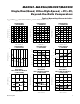
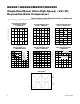
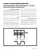
5) Refer to Figure 5 for a recommended circuit layout.
6) For slow-moving input signals, take care to prevent
parasitic feedback. A small capacitor (1000pF or
less) placed between the inputs can help eliminate
oscillations in the transition region. This capacitor
causes negligible degradation to t
PD
when the
source impedance is low.
Figure 4. Output Stage Circuitry
MAX961-MAX964
MAX997
MAX999
I
SOURCE
Q, Q
V
CC
GND
I
SINK
Figure 5. MAX961 PCB Layout
MAX961–MAX964/MAX997/MAX999
10
Maxim Integrated