
Datasheet


ELECTRICAL CHARACTERISTICS
(V
CC
= +2.7V to +5.5V, V
CM
= 0V, C
OUT
= 5pF, V
SHDN
= 0V, V
LE
= 0V, unless otherwise noted. T
MIN
to T
MAX
is -40°C to +85°C for all
E grade devices. For MAX999AAUK only, T
MIN
to T
MAX
is -40°C to +125°C.) (Note 1)
Single/Dual/Quad, Ultra-High-Speed, +3V/+5V,
Beyond-the-Rails Comparators
ABSOLUTE MAXIMUM RATINGS
Stresses beyond those listed under “Absolute Maximum Ratings” may cause permanent damage to the device. These are stress ratings only, and functional
operation of the device at these or any other conditions beyond those indicated in the operational sections of the specifications is not implied. Exposure to
absolute maximum rating conditions for extended periods may affect device reliability.
Supply Voltage, V
CC
to GND................................... -0.3V to +6V
All Other Pins..............................................-0.3V to (V
CC
+ 0.3V)
Current into Input Pins ......................................................±20mA
Duration of Output Short Circuit to GND or V
CC
.......Continuous
Continuous Power Dissipation (T
A
= +70°C)
5-Pin SOT23 (derate 7.1mW/°C above +70°C).......571mW/°C
8-Pin SO (derate 5.88mW/°C above +70°C)...........471mW/°C
8-Pin µMAX (derate 4.10mW/°C above +70°C) ......330mW/°C
14-Pin SO (derate 8.33mW/°C above +70°C).........667mW/°C
16-Pin SO (derate 8.70mW/°C above +70°C).........696mW/°C
16-Pin QSOP (derate 8.33mW/°C above +70°C)....667mW/°C
Operating Temperature Range
MAX96_E/MAX99_E.........................................-40°C to +85°C
MAX999AAUK ...............................................-40°C to +125°C
Storage Temperature Range ............................ -65°C to +160°C
Lead Temperature (soldering, 10s) .................................+300°C
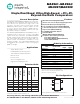
T
A
= +25°C T
MIN
to T
MAX
PARAMETER SYMBOL CONDITIONS
MIN TYP MAX MIN TYP MAX
UNITS
Supply Voltage V
CC
Inferred by PSRR 2.7 5.5 2.7 5.5 V
Input Common-Mode
Voltage Range
V
CMR
(Note 2) -0.1
V
CC
+
0.1
-0.1
V
CC
+
0.1
V
µMAX, SOT23 ±2.0 ±3.5 ±6.5
MAX999AAUK ±2.0 ±3.5 ±8.0
Input-Referred Trip Points V
TRIP
V
CM
= -0.1V
or 5.1V, V
CC
= 5V
(Note 3)
All other E
packages
±2.0 ±3.5 ±4.0
mV
Input-Referred Hysteresis 3.5 mV
µMAX, SOT23 ±0.5 ±1.5 ±4.5
MAX999AAUK ±0.5 ±1.5 ±6.0
Input Offset Voltage V
OS
V
CM
= -0.1V
or 5.1V, V
CC
= 5V
(Note 4)
All other E
packages
±0.5 ±1.5 ±2.0
mV
µMAX, SOT23 ±15 ±30
Input Bias Current I
B
V
IN+
= V
IN-
= 0V or V
CC
,
V
CC
= 5V
All other E
packages
±15 ±15
µA
Differential Input Clamp
Voltage
V
CC
= 5.5V, V
IN-
= 0V,
I
IN+
= 100µA
2.1 V
Input Capacitance 3 pF
Differential Input
Impedance
R
IND
V
CC
= 5V 8 kΩ
Common-Mode Input
R
INCM
V
CC
= 5V 130 kΩ
MAX961–MAX964/MAX997/MAX999
2
Maxim Integrated