
Datasheet


Single/Dual/Quad, Ultra-High-Speed, +3V/+5V,
Beyond-the-Rails Comparators
Note 1: The MAX961EUA/MAX962EUA/MAX997EUA/MAX999EUK are 100% production tested at T
A
= +25°C; all temperature specifica-
tions are guaranteed by design.
Note 2: Inferred by CMRR. Either input can be driven to the absolute maximum limit without false output inversion, provided that the other
input is within the input voltage range.
Note 3: The input-referred trip points are the extremities of the differential input voltage required to make the comparator output change
state. The difference between the upper and lower trip points is equal to the width of the input-referred hysteresis zone. (See
Figure 1.)
Note 4: Input offset voltage is defined as the mean of the trip points.
Note 5: CMRR = (V
OSL
- V
OSH
) / 5.2V, where V
OSL
is the offset at V
CM
= -0.1V and V
OSH
is the offset at V
CM
= 5.1V.
Note 6: PSRR = (V
OS
2.7 - V
OS
5.5) / 2.8V, where V
OS
2.7 is the offset voltage at V
CC
= 2.7V, and V
OS
5.5 is the offset voltage at
V
CC
= 5.5V.
Note 7: Propagation delay for these high-speed comparators is guaranteed by design characterization because it cannot be accurately
measured using automatic test equipment. A statistically significant sample of devices is characterized with a 200mV step and
100mV overdrive over the full temperature range. Propagation delay can be guaranteed by this characterization, since DC tests
ensure that all internal bias conditions are correct. For low overdrive conditions, V
TRIP
is added to the overdrive.
Note 8: Guaranteed by design.
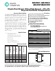
ELECTRICAL CHARACTERISTICS (continued)
(V
CC
= +2.7V to +5.5V, V
CM
= 0V, C
OUT
= 5pF, V
SHDN
= 0V, V
LE
= 0V, unless otherwise noted. T
MIN
to T
MAX
is -40°C to +85°C for all
E grade devices. For MAX999AAUK only, T
MIN
to T
MAX
is -40°C to +125°C.) (Note 1)
T
A
= +25°C T
MIN
to T
MAX
PARAMETER SYMBOL CONDITIONS
MIN TYP MAX MIN TYP MAX
UNITS
Data-to-Latch Setup Time t
SU
MAX961/MAX963 (Note 8) 5 5 ns
Latch-to-Data Hold Time t
H
MAX961/MAX963 (Note 8) 5 5 ns
Latch Pulse Width t
LPW
MAX961/MAX963 (Note 8) 5 5 ns
Latch Propagation Delay t
LPD
MAX961/MAX963 (Note 8) 10 10 ns
Shutdown Time t
OFF
Delay until output is high-Z
(> 10kΩ)
150 ns
Shutdown Disable Time t
ON
Delay until output is valid 250 ns
MAX961–MAX964/MAX997/MAX999
4
Maxim Integrated