
Operating instructions

Use an oscilloscope to verify that the conversion-start
signal is being strobed. Verify that SHDN is being dri-
ven high.
Problem: Unacceptable errors when measuring a
transducer.
Although most signal sources can be connected directly
to the MAX1132’s analog input, some high-impedance
signal sources may require an input buffer. Check for
settling errors by increasing the acquisition time: operate
the evaluation kit in external clock mode, 32 clocks per
conversion, with the QSPI clock at its slowest setting.
Problem: Measurements are erratic, unstable; poor
accuracy.
Check the reference voltage and input using a digital
voltmeter. Use an oscilloscope to check for noise.
When probing for noise, keep the oscilloscope ground
Evaluate: MAX1132/MAX1133
MAX1132 Evaluation Kit/Evaluation System
_______________________________________________________________________________________ 5
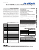
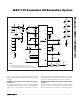
JU3
120
19
18
16
14
13
12
11
15
17
REF
REFADJ
AGND
AV
DD
DVDD AVDD
AVDD
DGND
AVDD
SHDN
P1
P0
P2
SSTRB
AIN
AGND
CREF
CS
DIN
DV
DD
DVDD
DVDD
DGND
SCLK
RST
DOUT
C3
2.2µF
10V
MAX1132
C2
10µF
10V
C1
10µF
10V
2
3
4
5
6
8
9
4321
7
10
C4
0.22µF
C7
1.0µF
C6
0.1µF
C5
0.1µF
JU4
JU2
TB1
FB2
DVDDTP1-2
J1-29
J1-7
1
2
JU1
3
DVDD
TB2
DVDD
C8
0.1µF
1
2
JU5
3
TP1-4
TP1-5
J1-38
J1-36
TP1-6
J1-37
TP1-7
J1-31
TP1-8U2-A U2-B
74HC04
U2-C
74HC04
56
U2-D
74HC04
98
U2-F
74HC04
11 10
U2-G
74HC04
13 12
74HC04
J1-35
TP1-3
J1-27
NOTES:
1. MINIMIZE PARASITIC CAPACITANCE OF U1 PIN 11–U2 PIN 1.
KEEP THE TRACE SHORT AND KEEP GROUND PLANE 0.025in AWAY.
2. U2 SUPPLY AND GROUND RETURN SHOULD BE ROUTED TO CONNECTOR J1, NOT FLOODED.
FB1
J1-8
J1-1
J1-2
J1-3
J1-4
TP1-1
TP1-2
R1
100kΩ
Figure 1. MAX1132 EV Kit Schematic Diagram