
User Manual


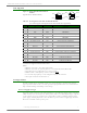


Table Of Contents
- 1. XBee®/XBee-PRO® RF Modules
- 2. RF Module Operation
- 3. RF Module Configuration
- Programming the RF Module
- Remote Configuration Commands
- Command Reference Tables
- Command Descriptions
- A1 (End Device Association) Command
- A2 (Coordinator Association) Command
- AC (Apply Changes) Command
- AI (Association Indication) Command
- AP (API Enable) Command
- AS (Active Scan) Command
- BD (Interface Data Rate) Command
- CA (CCA Threshold) Command
- CC (Command Sequence Character) Command
- CE (Coordinator Enable) Command
- CH (Channel) Command
- CN (Exit Command Mode) Command
- CT (Command Mode Timeout) Command
- D0 - D4 (DIOn Configuration) Commands
- D5 (DIO5 Configuration) Command
- D6 (DIO6 Configuration) Command
- D7 (DIO7 Configuration) Command
- D8 (DI8 Configuration) Command
- DA (Force Disassociation) Command
- DB (Received Signal Strength) Command
- DH (Destination Address High) Command
- DL (Destination Address Low) Command
- DN (Destination Node) Command
- DP (Disassociation Cyclic Sleep Period) Command
- EA (ACK Failures) Command
- EC (CCA Failures) Command
- ED (Energy Scan) Command
- EE (AES Encryption Enable) Command
- FP (Force Poll) Command
- FR (Software Reset) Command
- GT (Guard Times) Command
- HV (Hardware Version) Command
- IA (I/O Input Address) Command
- IC (DIO Change Detect) Command
- ID (Pan ID) Command
- IO (Digital Output Level) Command
- IR (Sample Rate) Command
- IS (Force Sample) Command
- IT (Samples before TX) Command
- IU (I/O Output Enable) Command
- KY (AES Encryption Key) Command
- M0 (PWM0 Output Level) Command
- M1 (PWM1 Output Level) Command
- MM (MAC Mode) Command
- MY (16-bit Source Address) Command
- NB (Parity) Command
- ND (Node Discover) Command
- NI (Node Identifier) Command
- NO (Node Discover Options) Command
- NT (Node Discover Time) Command
- P0 (PWM0 Configuration) Command
- P1 (PWM1 Configuration) Command
- PL (Power Level) Command
- PR (Pull-up Resistor) Command
- PT (PWM Output Timeout) Command
- RE (Restore Defaults) Command
- RN (Random Delay Slots) Command
- RO (Packetization Timeout) Command
- RP (RSSI PWM Timer) Command
- RR (XBee Retries) Command
- SC (Scan Channels) Command
- SD (Scan Duration) Command
- SH (Serial Number High) Command
- SL (Serial Number Low) Command
- SM (Sleep Mode) Command
- SO (Sleep Mode Command)
- SP (Cyclic Sleep Period) Command
- ST (Time before Sleep) Command
- T0 - T7 ((D0-D7) Output Timeout) Command
- VL (Firmware Version - Verbose)
- VR (Firmware Version) Command
- WR (Write) Command
- API Operation
- Appendix A: Agency Certifications
- Appendix B. Additional Information

XBee®/XBee‐PRO®RFModules‐802.15.4‐v1.xEx[2011.06.1]
©2011DigiInternatonal,Inc. 7
Pin Signals
Figure1‐03. XBee®/XBee‐PRO®RFModulePin
Numbers
(topsidesshown‐shieldsonbottom)
*Functionisnotsupportedatthetimeofthisrelease
Notes:
• Minimum connections: VCC, GND, DOUT & DIN
• Minimum connections for updating firmware: VCC, GND, DIN, DOUT, RTS & DTR
• Signal Direction is specified with respect to the module
• Module includes a 50k pull-up resistor attached to RESET
• Several of the input pull-ups can be configured using the PR command
• Unused pins should be left disconnected
Design Notes
The XBee modules do not specifically require any external circuitry or specific connections for
proper operation. However, there are some general design guidelines that are recommended for
help in troubleshooting and building a robust design.
Power Supply Design
Poor power supply can lead to poor radio performance, especially if the supply voltage is not kept
within tolerance or is excessively noisy. To help reduce noise, we recommend placing a 1.0 µF and
8.2 pF capacitor as near as possible to pin 1 on the XBee. If using a switching regulator for the
power supply, switching frequencies above 500 kHz are preferred. Power supply ripple should be
limited to a maximum 100 mV peak to peak.
Table1‐02. PinAssignmentsfortheXBeeandXBee‐PROModules
(Low‐assertedsignalsaredistinguishedwithahorizontallineabovesignalname.)
Pin # Name Direction Description
1 VCC - Power supply
2 DOUT Output UART Data Out
3 DIN / CONFIG
Input UART Data In
4 DO8* Output Digital Output 8
5 RESET
Input Module Reset (reset pulse must be at least 200 ns)
6 PWM0 / RSSI Output PWM Output 0 / RX Signal Strength Indicator
7 PWM1 Output PWM Output 1
8 [reserved] - Do not connect
9DTR
/ SLEEP_RQ / DI8 Input Pin Sleep Control Line or Digital Input 8
10 GND - Ground
11 AD4 / DIO4 Either Analog Input 4 or Digital I/O 4
12 CTS
/ DIO7 Either Clear-to-Send Flow Control or Digital I/O 7
13 ON / SLEEP
Output Module Status Indicator
14 VREF Input Voltage Reference for A/D Inputs
15 Associate / AD5 / DIO5 Either Associated Indicator, Analog Input 5 or Digital I/O 5
16 RTS
/ AD6 / DIO6 Either Request-to-Send Flow Control, Analog Input 6 or Digital I/O 6
17 AD3 / DIO3 Either Analog Input 3 or Digital I/O 3
18 AD2 / DIO2 Either Analog Input 2 or Digital I/O 2
19 AD1 / DIO1 Either Analog Input 1 or Digital I/O 1
20 AD0 / DIO0 Either Analog Input 0 or Digital I/O 0
Pin 1
Pin 10
Pin 1
Pin 10
Pin 20
Pin 11
Pin 20
Pin 11