PCI-2513 User's Guide Document Revision 3, June, 2007 © Copyright 2007, Measurement Computing Corporation
Your new Measurement Computing product comes with a fantastic extra — Management committed to your satisfaction! Refer to www.mccdaq.com/execteam.html for the names, titles, and contact information of each key executive at Measurement Computing. Thank you for choosing a Measurement Computing product—and congratulations! You own the finest, and you can now enjoy the protection of the most comprehensive warranties and unmatched phone tech support.
Trademark and Copyright Information TracerDAQ, Universal Library, Harsh Environment Warranty, Measurement Computing Corporation, and the Measurement Computing logo are either trademarks or registered trademarks of Measurement Computing Corporation. Windows, Microsoft, and Visual Studio are either trademarks or registered trademarks of Microsoft Corporation LabVIEW is a trademark of National Instruments. CompactFlash is a registered trademark of SanDisk Corporation.
Table of Contents Preface About this User's Guide .......................................................................................................................7 What you will learn from this user's guide .........................................................................................................7 Conventions used in this user's guide .................................................................................................................7 Where to find more information ......
PCI-2513 User's Guide What are detection setpoints? ..........................................................................................................................................24 Setpoint configuration overview ......................................................................................................................................24 Setpoint configuration...............................................................................................................................
Preface About this User's Guide What you will learn from this user's guide This user's guide explains how to install, configure, and use the PCI-2513 so that you get the most out of its analog input, digital I/O, and counter/timer I/O features. This user's guide also refers you to related documents available on our web site, and to technical support resources.
Chapter 1 Introducing the PCI-2513 Overview: PCI-2513 features The PCI-2513 is supported under popular Microsoft® Windows® operating systems. The PCI-2513 provides either eight differential or 16 single-ended analog inputs with 16-bit resolution. It offers seven software-selectable analog input ranges of ±10 V, ±5 V, ±2 V, ±1 V, ±0.5 V, ±0.2 V, and ±0.1V. The board has 24 high-speed lines of digital I/O, two timer outputs, and four 32-bit counters.
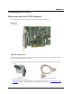
Chapter 2 Installing the PCI-2513 What comes with your PCI-2513 shipment? As you unpack your PCI-2513, verify that the following components are included. Hardware PCI-2513 Optional components Cables and signal conditioning accessories that are compatible with the PCI-2513 are not included with PCI2513 orders, and must be ordered separately. If you ordered any of the following products with your board, they should be included with your shipment.
PCI-2513 User's Guide Installing the PCI-2513 Additional documentation In addition to this hardware user's guide, you should also receive the Quick Start Guide (available in PDF at www.mccdaq.com/PDFmanuals/DAQ-Software-Quick-Start.pdf). This booklet supplies a brief description of the software you received with your PCI-2513 and information regarding installation of that software. Please read this booklet completely before installing any software or hardware.
PCI-2513 User's Guide 3. Installing the PCI-2513 To test your installation and configure your board, run the InstaCal utility installed in the previous section. Refer to the Quick Start Guide that came with your board for information on how to initially set up and load InstaCal. If your board has been powered-off for more than 10 minutes, allow your computer to warm up for at least 30 minutes before acquiring data. This warm-up period is required in order for the board to achieve its rated accuracy.
PCI-2513 User's Guide Installing the PCI-2513 Pinout – main I/O connector 16-channel single-ended pin out (8-channel differential signals in parentheses) Signal name Pin ACH0 (ACH0 HI) AGND ACH9 (ACH1 LO) ACH2 (ACH2 HI) AGND ACH11 (ACH3 LO) SGND ACH12 (ACH4 LO) ACH5 (ACH5 HI) AGND ACH14 (ACH6 LO) ACH7 (ACH7 HI) NC NC NEGREF (reserved for self-calibration) GND A1 A3 A5 A7 B1 B3 B5 B7 C1 C3 C5 C7 GND CNT1 CNT3 TMR1 GND GND PCI slot ↓ 68 67 66 65 64 63 62 61 60 59 58 57 56 55 54 53 52 51 50 49 48 47 46 45
PCI-2513 User's Guide Installing the PCI-2513 34 68 1 35 34 68 1 35 Figure 2. CA-68-3S and CA-68-6S cable Field wiring and signal termination You can use the following MCC screw terminal boards to terminate field signals and route them into the PCI2513 board using the CA-68-3R, CA-68-3S, or CA-68-6S cable: TB-100: Termination board with screw terminals. Details on this product are available on our web site at www.mccdaq.com/cbicatalog/cbiproduct.asp?dept_id=98&pf_id=1787.
Chapter 3 Functional Details This chapter contains detailed information on all of the features available from the board, including: a block diagram of board functions information on how to use, when to use, and when not to use the signals generated by the board diagrams of signals using default or conventional board settings PCI-2513 block diagram Figure 3 is a simplified block diagram of the PCI-2513. This board provides all of the functional elements shown in the figure. Figure 3.
PCI-2513 User's Guide Functional Details Bus mastering DMA The PCI-2513 supports bus mastering DMA. With multiple DMA channels, analog, digital, and counter input data, as well as digital output data, can flow between the PC and the PCI-2513 without consuming valuable CPU time. The driver supplied with the PCI-2513 automatically uses bus mastering DMA to efficiently conduct I/O from the PC to the PCI-2513.
PCI-2513 User's Guide Functional Details Digital I/O Twenty-four TTL-level digital I/O lines are included in each PCI-2513. You can program digital I/O in 8-bit groups as either inputs or outputs and scan them in several modes (see "Digital input scanning" below). You can access input ports asynchronously from the PC at any time, including when a scanned acquisition is occurring. Digital input scanning Digital input ports can be read asynchronously before, during, or after an analog input scan.
PCI-2513 User's Guide Functional Details 3. Bring the analog input signal toward the desired threshold. When the input signal is at the threshold (± some tolerance) the sweep will be triggered. 4. Before re-arming the trigger, again move the analog input signal to a level that is more than 2.5% of the full-scale range away from the desired threshold.
PCI-2513 User's Guide Functional Details Pre-triggering and post-triggering modes The PCI-2513 supports four modes of pre-triggering and post-triggering, providing a wide-variety of options to accommodate any measurement requirement. When using pre-trigger, you must use software-based triggering to initiate an acquisition. No pre-trigger, post-trigger stop event. In this simple mode, data acquisition starts when the trigger is received, and the acquisition stops when the stoptrigger event is received.
PCI-2513 User's Guide Functional Details Mapped channels A mapped channel is one of four counter input signals that can get multiplexed into a counter module. The mapped channel can participate with the counter's input signal by gating the counter, latching the counter, and so on. The four possible choices for the mapped channel are the four counter input signals (post-debounce).
PCI-2513 User's Guide Functional Details Gating "on" mode Sets the gating option to "on" for the mapped channel, enabling the mapped channel to gate the counter. Any counter can be gated by the mapped channel. When the mapped channel is high, the counter is enabled. When the mapped channel is low, the counter is disabled (but holds the count value). The mapped channel can be any counter input channel other than the counter being gated.
PCI-2513 User's Guide Functional Details Figure 7. Debounce module – trigger after stable mode The following time periods (T1 through T5) pertain to Figure 7. In trigger after stable mode, the input signal to the debounce module is required to have a period of stability after an incoming edge, in order for that edge to be accepted (passed through to the counter module.) The debounce time for this example is equal to T2 and T5.
PCI-2513 User's Guide Functional Details Debounce mode comparisons Figure 9 shows how the two modes interpret the same input signal, which exhibits glitches. Notice that the trigger before stable mode recognizes more glitches than the trigger after stable mode. Use the bypass option to achieve maximum glitch recognition. Figure 9. Example of two debounce modes interpreting the same signal Debounce times should be set according to the amount of instability expected in the input signal.
PCI-2513 User's Guide Functional Details Figure 11. Optimal debounce time for trigger after stable mode Timer outputs Two 16-bit timer outputs are built into every 3000 series board. Each timer is capable of generating a different square wave with a programmable frequency in the range of 16 Hz to 1 MHz. Figure 12. Typical PCI-2513 timer channel Example: Timer outputs Timer outputs are programmable square waves. The period of the square wave can be as short as 1us or as long as 65535 µs.
PCI-2513 User's Guide Functional Details Using detection setpoints for output control What are detection setpoints? With the PCI-2513's setpoint configuration feature, you can configure up to 16 detection setpoints associated with channels in a scan group.
PCI-2513 User's Guide Functional Details Action - driven by condition Compare X to: Setpoint definition (choose one) Limit A or Limit B Equal to A (X = A) Below A (X < A) Above B (X > B) Window* (nonhysteresis mode) Inside (B < X < A) Outside: B > X; or, X > A Window* (hysteresis mode) Above A (X > A) Below (B X < B) (Both conditions are checked when in hysteresis mode Update conditions: True only: If True, then output value 1 If False, then perform no action True and False: I
PCI-2513 User's Guide Functional Details Setpoint configuration You program all setpoints as part of the pre-acquisition setup, similar to setting up an external trigger. Since each setpoint acts on 16-bit data, each has two 16-bit compare values: a high limit (limit A) and a low limit (limit B). These limits define the setpoint window. There are several possible conditions (criteria) and effectively three update modes, as explained in the following configuration summary.
PCI-2513 User's Guide Functional Details Using the setpoint status register You can use the setpoint status register to check the current state of the 16 possible setpoints. In the register, Setpoint 0 is the least-significant bit and Setpoint 15 is the most-significant bit. Each setpoint is assigned a value of 0 or 1. A value of 0 indicates that the setpoint criteria is not met—in other words, the condition is False.
PCI-2513 User's Guide Functional Details You can program control outputs programmed on each setpoint, and use the detection for channel 4 to update the FIRSTPORTC digital output port with one value (70 h in the example) when the analog input voltage is within the shaded region and a different value when the analog input voltage is outside the shaded region (30 h in the example).
PCI-2513 User's Guide Functional Details Figure 16. Channel 3 in hysteresis mode Detecting setpoints on a totalizing counter In the following figure, Channel 1 is a counter in totalize mode. Two setpoints define a point of change for Detect 1 as the counter counts upward. The detect output is high when inside the window (greater than Limit B (the low limit) but less than Limit A (the high limit). In this case, the Channel 1 setpoint is defined for the 16 lower bits of channel 1's 32-bit value.
PCI-2513 User's Guide Functional Details inside the window. There is one update value that gets applied when the input values are less than the window and a different update value that gets applied when the input values are greater than the window. Update on True and False uses two update values. The update values can drive FIRSTPORTC or timer outputs. FIRSTPORTC digital outputs can be updated immediately upon setpoint detection.
PCI-2513 User's Guide Functional Details There are three possible solutions for overcoming this problem: Shorten the scan period to give more timing resolution on the counter values or analog values. Widen the setpoint window by increasing limit A and/or lowering limit B. A combination of both solutions (1 and 2) could be made.
Chapter 4 Calibrating the PCI-2513 Every range of a PCI-2513 device is calibrated at the factory using a digital NIST traceable calibration method. This method works by storing a correction factor for each range on the unit at the time of calibration. For analog inputs, the user can adjust the calibration of the board while it is installed in the acquisition system. This does not destroy the factory calibration supplied with the board.
Chapter 5 Specifications Typical for 25 °C unless otherwise specified. Specifications in italic text are guaranteed by design. Analog input Table 1.
PCI-2513 User's Guide Specifications Digital input / output Table 3. Digital input/output specifications Number of I/O Ports Input scanning mode Configuration Input protection Input high Input low Output high Output low Output current Digital input pacing Digital output pacing Digital input trigger sources and modes Digital output trigger sources Data transfer Sampling/update rate Pattern generation output 24 Three banks of 8.
PCI-2513 User's Guide Specifications Input sequencer Analog, digital, and counter inputs can be scanned based on either an internal programmable timer or an external clock source. Table 5. Input sequencer specifications Scan clock sources: two (Note 3) Programmable parameters per scan Depth Onboard channel-to-channel scan rate External acquisition scan clock input maximum rate Clock signal range: Minimum pulse width Note 3: Internal: Analog channels from 1 µs to 1 sec in 20.83 ns steps.
PCI-2513 User's Guide Specifications Frequency/pulse generators Table 7. Frequency/pulse generator specifications Channels Output waveform Output rate High-level output voltage Low-level output voltage 2 x 16-bit Square wave 1 MHz base rate divided by 1 to 65535 (programmable) 2.0 V minimum @ -1.0 mA, 2.9 V minimum @ -400 µA 0.4 V maximum @ 400 µA Power consumption Table 8. Power consumption specifications Power consumption (per board) 3W PCI compatibility Table 9.
PCI-2513 User's Guide Specifications Table 13.
PCI-2513 User's Guide Specifications Table 14.
Declaration of Conformity Manufacturer: Address: Category: IOTech, Incorporated 25971 Cannon Road Cleveland, OH 44146 USA Information technology equipment.
Measurement Computing Corporation 10 Commerce Way Suite 1008 Norton, Massachusetts 02766 (508) 946-5100 Fax: (508) 946-9500 E-mail: info@mccdaq.com www.mccdaq.