
Product Description


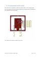
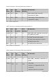

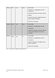
Table Of Contents
- 1 General Information / Security Advice
- 2 Product Description
- 3 RFID Integration Guide
- 3.1 General Hints
- 3.2 List of applicable FCC rules and ISED radio standards
- 3.3 Specific operational use conditions
- 3.4 Limited module procedures
- 3.5 Trace antenna designs
- 3.6 RF exposure considerations
- 3.7 Antennas
- 3.8 Label and compliance information
- 3.9 Information on test modes and additional testing requirements
- 3.10 Additional testing, Part 15 Subpart B disclaimer
- 4 Power Supply and Power Consumption
- 5 Communication
- 6 Digital Inputs / Outputs (GPIOs)
- 7 Certification
- 8 Further Notes
- 9 Version History

$22..D"
Pin
Name
Pin
Nr.
Pin
Direction
PCB Pin
Marking
Pin Function
$H&* D" $B >F@ .2..)&*<)
&H&*
J! D" $B >J@ ..)<2
!..)
!
+..D"
Pin
Name
Pin
Nr.
Pin
Direction
PCB
Marking
Pin Function
+H&* D" $" >&@ +&*<*4)
$H&*&H&*
D D" >@ !+.
4.
,2./
D D"# >@ !+.
"#$$
&$4..D#"
Pin
Name
Pin
Nr.
Pin
Direction
PCB
Marking
Pin Function
&H&* D#" $" >&@ &$4 &*< )
$H&*
&$4H
D#" '4
#"#!&$4<
/:B
<
C<
$7%