PIC16F72X/PIC16LF72X Data Sheet 28/40/44-Pin Flash Microcontrollers with nanoWatt XLP Technology © 2009 Microchip Technology Inc.
Note the following details of the code protection feature on Microchip devices: • Microchip products meet the specification contained in their particular Microchip Data Sheet. • Microchip believes that its family of products is one of the most secure families of its kind on the market today, when used in the intended manner and under normal conditions. • There are dishonest and possibly illegal methods used to breach the code protection feature.
PIC16F72X/PIC16LF72X 28/40/44-Pin Flash Microcontrollers with nanoWatt XLP Technology Devices Included In This Data Sheet: PIC16F72X Devices: • PIC16F722 • PIC16F726 • PIC16F723 • PIC16F727 Extreme Low-Power Management PIC16LF72X with nanoWatt XLP: • Sleep Mode: 20 nA • Watchdog Timer: 500 nA • Timer1 Oscillator: 600 nA @ 32 kHz • PIC16F724 Analog Features: PIC16LF72X Devices: • PIC16LF722 • PIC16LF726 • PIC16LF723 • PIC16LF727 • PIC16LF724 High-Performance RISC CPU: • Only 35 Instructions to Le
PIC16F72X/PIC16LF72X Device PIC16F722/ PIC16LF722 PIC16F723/ PIC16LF723 PIC16F724/ PIC16LF724 PIC16F726/ PIC16LF726 PIC16F727/ PIC16LF727 DS41341E-page 4 Program Memory Flash (words) SRAM (bytes) I/Os Interrupts 8-bit A/D (ch) AUSART CCP Timers 8/16-bit 2048 128 25 12 11 Yes 2 2/1 4096 192 25 12 11 Yes 2 2/1 4096 192 36 12 14 Yes 2 2/1 8192 368 25 12 11 Yes 2 2/1 8192 368 36 12 14 Yes 2 2/1 © 2009 Microchip Technology Inc.
PIC16F72X/PIC16LF72X Pin Diagrams – 28-PIN PDIP/SOIC/SSOP/QFN/UQFN (PIC16F722/723/726/PIC16LF722/723/726) PDIP, SOIC, SSOP 1 28 RB7/ICSPDAT 2 27 RB6/ICSPCLK AN1/RA1 3 26 RB5/AN13/CPS5/T1G AN2/RA2 4 25 RB4/AN11/CPS4 24 23 RB3/AN9/CPS3/CCP2(1) VREF/AN3/RA3 5 T0CKI/CPS6/RA4 6 VCAP(3)/SS(2)/CPS7/AN4/RA5 7 VSS 8 CLKIN/OSC1/RA7 9 PIC16F722/723/726/ PIC16LF722/723/726 VPP/MCLR/RE3 VCAP(3)/SS(2)/AN0/RA0 RB2/AN8/CPS2 22 21 RB1/AN10/CPS1 RB0/AN12/CPS0/INT 20 VDD 19 (1) CCP2 /T1OSI/R
PIC16F72X/PIC16LF72X TABLE 1: 28-PIN PDIP/SOIC/SSOP/QFN/UQFN SUMMARY (PIC16F722/723/726/PIC16LF722/723/726) I/O 28-Pin PDIP, SOIC, SSOP 28-Pin QFN, UQFN A/D Cap Sensor Timers CCP AUSART SSP RA0 2 27 AN0 — — — — SS(3) — — VCAP(4) RA1 3 28 AN1 — — — — — — — — RA2 4 1 AN2 — — — — — — — — RA3 5 2 AN3/VREF — — — — — — — — Interrupt Pull-Up Basic RA4 6 3 — CPS6 T0CKI — — — — — — RA5 7 4 AN4 CPS7 — — — SS(3) — — VCAP(4) RA6 10 7
PIC16F72X/PIC16LF72X Pin Diagrams – 40-PIN PDIP (PIC16F724/727/PIC16LF724/727) VPP/MCLR/RE3 (3) 1 40 RB7/ICSPDAT VCAP /SS /AN0/RA0 2 39 RB6/ICSPCLK AN1/RA1 3 38 RB5/AN13/CPS5/T1G AN2/RA2 4 37 RB4/AN11/CPS4 VREF/AN3/RA3 5 36 RB3/AN9/CPS3/CCP2(1) T0CKI/CPS6/RA4 6 35 RB2/AN8/CPS2 /CPS7/AN4/RA5 AN5/RE0 7 34 33 RB1/AN10/CPS1 RB0/AN12/CPS0/INT AN6/RE1 9 32 VDD AN7/RE2 10 31 VSS VDD 11 30 RD7/CPS15 VSS 12 29 RD6/CPS14 (3) /SS (2) 8 PIC16F724/727/ PIC16LF724/727 VCA
PIC16F72X/PIC16LF72X 44 43 42 41 40 39 38 37 36 35 34 RC6/TX/CK RC5/SDO RC4/SDI/SDA RD3/CPS11 RD2/CPS10 RD1/CPS9 RD0/CPS8 RC3/SCK/SCL RC2/CCP1 RC1/T1OSI/CCP2(1) NC Pin Diagrams – 44-PIN TQFP (PIC16F724/727/PIC16LF724/727) PIC16F724/727/ PIC16LF724/727 33 32 31 30 29 28 27 26 25 24 23 NC RC0/T1OSO/T1CKI RA6/OSC2/CLKOUT/VCAP(3) RA7/OSC1/CLKIN VSS VDD RE2/AN7 RE1/AN6 RE0/AN5 RA5/AN4/CPS7/SS(2)/VCAP(3) RA4/CPS6/T0CKI NC NC CPS4/AN11/RB4 T1G/CPS5/AN13/RB5 ICSPCLK/RB6 ICSPDAT/RB7 VPP/MCLR/RE3 VCAP(3)/SS(2)
PIC16F72X/PIC16LF72X PIC16F724/727/ PIC16LF724/727 33 32 31 30 29 28 27 26 25 24 23 12 13 14 15 16 17 18 19 20 21 22 1 2 3 4 5 6 7 8 9 10 11 RA6/OSC2/CLKOUT/VCAP(3) RA7/OSC1/CLKIN VSS VSS NC VDD RE2/AN7 RE1/AN6 RE0/AN5 RA5/AN4/CPS7/SS(2)/VCAP(3) RA4/CPS6/T0CKI CCP2(1)/CPS3/AN9/RB3 NC CPS4/AN11/RB4 T1G/CPS5/AN13/RB5 ICSPCLK/RB6 ICSPDAT/RB7 VPP/MCLR/RE3 VCAP(3)/SS(2)/AN0/RA0 AN1/RA1 AN2/RA2 VREF/AN3/RA3 DT/RX/RC7 CPS12/RD4 CPS13/RD5 CPS14/RD6 CPS15/RD7 VSS VDD VDD INT/CPS0/AN12/RB0 CPS1/AN10/RB1 CPS2/A
PIC16F72X/PIC16LF72X 40/44-PIN PDIP/TQFP/QFN SUMMARY (PIC16F724/727/PIC16LF724/727) TABLE 2: I/O 40-Pin PDIP 44-Pin TQFP 44-Pin QFN A/D Cap Sensor Timers CCP AUSART SSP RA0 2 19 19 AN0 — — — — SS(3) — — VCAP(4) RA1 3 20 20 AN1 — — — — — — — — RA2 4 21 21 AN2 — — — — — — — — RA3 5 22 22 AN3/VREF — — — — — — — — RA4 6 23 23 — CPS6 T0CKI — — — — — — RA5 7 24 24 AN4 CPS7 — — — SS(3) — — VCAP(4) RA6 14 31 33 — — — —
PIC16F72X/PIC16LF72X Table of Contents 1.0 Device Overview ....................................................................................................................................................................... 13 2.0 Memory Organization ................................................................................................................................................................ 19 3.0 Resets ...................................................................................
PIC16F72X/PIC16LF72X TO OUR VALUED CUSTOMERS It is our intention to provide our valued customers with the best documentation possible to ensure successful use of your Microchip products. To this end, we will continue to improve our publications to better suit your needs. Our publications will be refined and enhanced as new volumes and updates are introduced.
PIC16F72X/PIC16LF72X 1.0 DEVICE OVERVIEW The PIC16F72X/PIC16LF72X devices are covered by this data sheet. They are available in 28/40/44-pin packages. Figure 1-1 shows a block diagram of the PIC16F722/723/726/PIC16LF722/723/726 devices and Figure 1-2 shows a block diagram of the PIC16F724/727/PIC16LF724/727 devices. Table 1-1 shows the pinout descriptions. © 2009 Microchip Technology Inc.
PIC16F72X/PIC16LF72X FIGURE 1-1: PIC16F722/723/726/PIC16LF722/723/726 BLOCK DIAGRAM PORTA Configuration 13 Program Counter Flash Program Memory Program Bus 8 Level Stack (13-bit) 14 RA0 RA1 RA2 RA3 RA4 RA5 RA6 RA7 8 Data Bus RAM PORTB 9 RAM Addr Addr MUX Instruction Instruction Reg reg 7 Direct Addr 8 Indirect Addr FSR FSR Reg reg STATUS STATUS Reg reg PORTC 8 3 Power-up Timer Oscillator Start-up Timer Instruction Decode Decodeand & Control Timing Generation OSC2/CLKOUT MUX PORTE 8
PIC16F72X/PIC16LF72X FIGURE 1-2: PIC16F724/727/PIC16LF724/727 BLOCK DIAGRAM PORTA Configuration 13 Program Counter Flash Program Memory Program Bus 8 Level Stack (13-bit) RA0 RA1 RA2 RA3 RA4 RA5 RA6 RA7 8 Data Bus RAM 14 PORTB 9 RAM Addr RB0 RB1 RB2 RB3 RB4 RB5 RB6 RB7 Addr MUX Instruction Instruction Reg reg 7 Direct Addr 8 Indirect Addr FSR reg Reg FSR STATUS STATUS Reg reg 8 3 Power-up Timer Instruction Decode Decodeand & Control OSC1/CLKIN OSC2/CLKOUT Timing Generation Internal Osc
PIC16F72X/PIC16LF72X TABLE 1-1: PIC16F72X/PIC16LF72X PINOUT DESCRIPTION Name RA0/AN0/SS/VCAP RA1/AN1 RA2/AN2 RA3/AN3/VREF RA4/CPS6/T0CKI RA5/AN4/CPS7/SS/VCAP RA6/OSC2/CLKOUT/VCAP RA7/OSC1/CLKIN RB0/AN12/CPS0/INT RB1/AN10/CPS1 RB2/AN8/CPS2 RB3/AN9/CPS3/CCP2 Function Input Type RA0 TTL AN0 AN — SS ST — Power Power RA1 TTL AN1 AN RA2 TTL AN2 AN RA3 TTL AN3 AN VREF AN RA4 TTL Description CMOS General purpose I/O. VCAP A/D Channel 0 input. Slave Select input.
PIC16F72X/PIC16LF72X TABLE 1-1: PIC16F72X/PIC16LF72X PINOUT DESCRIPTION (CONTINUED) Name RB4/AN11/CPS4 RB5/AN13/CPS5/T1G RB6/ICSPCLK/ICDCLK RB7/ICSPDAT/ICDDAT RC0/T1OSO/T1CKI RC1/T1OSI/CCP2 RC2/CCP1 RC3/SCK/SCL RC4/SDI/SDA RC5/SDO RC6/TX/CK RC7/RX/DT RD0/CPS8 RD1/CPS9 RD2/CPS10 Function Input Type RB4 TTL Description CMOS General purpose I/O. Individually controlled interrupt-on-change. Individually enabled pull-up. AN11 AN — A/D Channel 11 input.
PIC16F72X/PIC16LF72X TABLE 1-1: PIC16F72X/PIC16LF72X PINOUT DESCRIPTION (CONTINUED) Name RD3/CPS11 RD4/CPS12 RD5/CPS13 RD6/CPS14 RD7/CPS15 Function Input Type RD3 ST CPS11 AN RD4 ST CPS12 AN RD5 ST CPS13 AN RD6 ST CPS14 AN RD7 ST CPS15 AN RE0/AN5 RE0 ST AN5 AN RE1/AN6 RE1 ST AN6 AN RE2/AN7 RE2 ST RE3/MCLR/VPP Output Type Description CMOS General purpose I/O. — Capacitive sensing input 11. CMOS General purpose I/O. — Capacitive sensing input 12.
PIC16F72X/PIC16LF72X 2.0 MEMORY ORGANIZATION 2.1 Program Memory Organization The PIC16F72X/PIC16LF72X has a 13-bit program counter capable of addressing a 2K x 14 program memory space for the PIC16F722/LF722 (0000h-07FFh), a 4K x 14 program memory space for the PIC16F723/LF723 and PIC16F724/LF724 (0000h-0FFFh) and an 8K x 14 program memory space for the PIC16F726/LF726 and PIC16F727/LF727 (0000h-1FFFh).
PIC16F72X/PIC16LF72X FIGURE 2-3: PROGRAM MEMORY MAP AND STACK FOR THE PIC16F726/LF726 AND PIC16F727/LF727 PC<12:0> CALL, RETURN RETFIE, RETLW 13 Stack Level 1 Stack Level 2 Stack Level 8 Reset Vector 0000h Interrupt Vector 0004h 0005h Page 0 07FFh 0800h On-chip Program Memory 2.2 The data memory is partitioned into multiple banks which contain the General Purpose Registers (GPRs) and the Special Function Registers (SFRs). Bits RP0 and RP1 are bank select bits.
PIC16F72X/PIC16LF72X FIGURE 2-4: PIC16F722/LF722 SPECIAL FUNCTION REGISTERS File Address Indirect addr.(*) 00h Indirect addr.(*) 80h Indirect addr.(*) 100h Indirect addr.
PIC16F72X/PIC16LF72X FIGURE 2-5: PIC16F723/LF723 AND PIC16F724/LF724 SPECIAL FUNCTION REGISTERS File Address Indirect addr.(*) 00h Indirect addr.(*) 80h Indirect addr.(*) 100h Indirect addr.
PIC16F72X/PIC16LF72X FIGURE 2-6: PIC16F726/LF726 AND PIC16F727/LF727 SPECIAL FUNCTION REGISTERS File Address Indirect addr.(*) 00h Indirect addr.(*) 80h Indirect addr.(*) 100h Indirect addr.
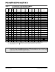
PIC16F72X/PIC16LF72X TABLE 2-1: Address Name PIC16F72X/PIC16LF72X SPECIAL FUNCTION REGISTER SUMMARY Bit 7 Bit 6 Bit 5 Bit 4 Bit 3 Bit 2 Bit 1 Bit 0 Value on: POR, BOR Page Bank 0 00h(2) INDF Addressing this location uses contents of FSR to address data memory (not a physical register) xxxx xxxx 31,40 01h TMR0 Timer0 Module Register xxxx xxxx 111,40 02h(2) PCL Program Counter (PC) Least Significant Byte 03h(2) STATUS IRP RP1 RP0 TO PD Z DC C 0000 0000 30,40 0001 1xxx 27,
PIC16F72X/PIC16LF72X TABLE 2-1: Address PIC16F72X/PIC16LF72X SPECIAL FUNCTION REGISTER SUMMARY (CONTINUED) Name Bit 7 Bit 6 Bit 5 Bit 4 Bit 3 Bit 2 Bit 1 Bit 0 Value on: POR, BOR Page Bank 1 80h(2) INDF 81h OPTION_REG 82h(2) PCL 83h(2) STATUS Addressing this location uses contents of FSR to address data memory (not a physical register) RBPU INTEDG T0CS xxxx xxxx 31,40 PSA PS2 PS1 PS0 1111 1111 28,41 0000 0000 30,40 TO PD Z DC C 0001 1xxx 27,40 T0SE Program Counter (
PIC16F72X/PIC16LF72X TABLE 2-1: Address PIC16F72X/PIC16LF72X SPECIAL FUNCTION REGISTER SUMMARY (CONTINUED) Name Bit 7 Bit 6 Bit 5 Bit 4 Bit 3 Bit 2 Bit 1 Bit 0 Value on: POR, BOR Page Bank 2 100h(2) INDF Addressing this location uses contents of FSR to address data memory (not a physical register) xxxx xxxx 31,40 101h TMR0 Timer0 Module Register xxxx xxxx 111,40 102h(2) PCL Program Counter’s (PC) Least Significant Byte 103h(2) STATUS 104h(2) FSR IRP RP1 RP0 TO PD Z DC C
PIC16F72X/PIC16LF72X 2.2.2.1 STATUS Register The STATUS register, shown in Register 2-1, contains: • the arithmetic status of the ALU • the Reset status • the bank select bits for data memory (SRAM) The STATUS register can be the destination for any instruction, like any other register. If the STATUS register is the destination for an instruction that affects the Z, DC or C bits, then the write to these three bits is disabled. These bits are set or cleared according to the device logic.
PIC16F72X/PIC16LF72X 2.2.2.2 OPTION register Note: The OPTION register, shown in Register 2-2, is a readable and writable register, which contains various control bits to configure: • • • • Timer0/WDT prescaler External RB0/INT interrupt Timer0 Weak pull-ups on PORTB REGISTER 2-2: To achieve a 1:1 prescaler assignment for Timer0, assign the prescaler to the WDT by setting PSA bit of the OPTION register to ‘1’. Refer to Section 12.3 “Timer1 Prescaler”.
PIC16F72X/PIC16LF72X 2.2.2.3 PCON Register The Power Control (PCON) register contains flag bits (refer to Table 3-2) to differentiate between a: • • • • Power-on Reset (POR) Brown-out Reset (BOR) Watchdog Timer Reset (WDT) External MCLR Reset The PCON register also controls the software enable of the BOR. The PCON register bits are shown in Register 2-3.
PIC16F72X/PIC16LF72X 2.3 PCL and PCLATH The Program Counter (PC) is 13 bits wide. The low byte comes from the PCL register, which is a readable and writable register. The high byte (PC<12:8>) is not directly readable or writable and comes from PCLATH. On any Reset, the PC is cleared. Figure 2-7 shows the two situations for the loading of the PC. The upper example in Figure 2-7 shows how the PC is loaded on a write to PCL (PCLATH<4:0> → PCH).
PIC16F72X/PIC16LF72X 2.5 EXAMPLE 2-2: Indirect Addressing, INDF and FSR Registers MOVLW MOVWF BANKISEL NEXT CLRF INCF BTFSS GOTO CONTINUE The INDF register is not a physical register. Addressing the INDF register will cause indirect addressing. Indirect addressing is possible by using the INDF register. Any instruction using the INDF register actually accesses data pointed to by the File Select Register (FSR). Reading INDF itself indirectly will produce 00h.
PIC16F72X/PIC16LF72X NOTES: DS41341E-page 32 © 2009 Microchip Technology Inc.
PIC16F72X/PIC16LF72X 3.0 RESETS The PIC16F72X/PIC16LF72X differentiates between various kinds of Reset: a) b) c) d) e) f) Power-on Reset (POR) WDT Reset during normal operation WDT Reset during Sleep MCLR Reset during normal operation MCLR Reset during Sleep Brown-out Reset (BOR) A simplified block diagram of the On-Chip Reset Circuit is shown in Figure 3-1. Some registers are not affected in any Reset condition; their status is unknown on POR and unchanged in any other Reset.
PIC16F72X/PIC16LF72X TABLE 3-1: STATUS BITS AND THEIR SIGNIFICANCE POR BOR TO PD 0 x 1 1 Power-on Reset or LDO Reset 0 x 0 x Illegal, TO is set on POR 0 x x 0 Illegal, PD is set on POR 1 0 1 1 Brown-out Reset 1 1 0 1 WDT Reset 1 1 0 0 WDT Wake-up 1 1 u u MCLR Reset during normal operation 1 1 1 0 MCLR Reset during Sleep or interrupt wake-up from Sleep TABLE 3-2: Condition RESET CONDITION FOR SPECIAL REGISTERS(2) Program Counter STATUS Register PCON Register
PIC16F72X/PIC16LF72X 3.1 MCLR 3.3 The PIC16F72X/PIC16LF72X has a noise filter in the MCLR Reset path. The filter will detect and ignore small pulses. It should be noted that a Reset does not drive the MCLR pin low. Voltages applied to the pin that exceed its specification can result in both MCLR Resets and excessive current beyond the device specification during the ESD event. For this reason, Microchip recommends that the MCLR pin no longer be tied directly to VDD.
PIC16F72X/PIC16LF72X 3.4.2 WDT CONTROL The WDTE bit is located in the Configuration Word Register 1. When set, the WDT runs continuously. The PSA and PS<2:0> bits of the OPTION register control the WDT period. See Section 11.0 “Timer0 Module” for more information.
PIC16F72X/PIC16LF72X 3.5 Brown-Out Reset (BOR) If VDD falls below VBOR for greater than parameter (TBOR) (see Section 23.0 “Electrical Specifications”), the Brown-out situation will reset the device. This will occur regardless of VDD slew rate. A Reset is not ensured to occur if VDD falls below VBOR for more than parameter (TBOR). Brown-out Reset is enabled by programming the BOREN<1:0> bits in the Configuration register.
PIC16F72X/PIC16LF72X 3.6 Time-out Sequence 3.7 On power-up, the time-out sequence is as follows: first, PWRT time-out is invoked after POR has expired, then OST is activated after the PWRT time-out has expired. The total time-out will vary based on oscillator configuration and PWRTE bit status. For example, in EC mode with PWRTE bit = 1 (PWRT disabled), there will be no time-out at all. Figure 3-4, Figure 3-5 and Figure 3-6 depict time-out sequences.
PIC16F72X/PIC16LF72X FIGURE 3-4: TIME-OUT SEQUENCE ON POWER-UP (DELAYED MCLR): CASE 1 VDD MCLR Internal POR TPWRT PWRT Time-out TOST OST Time-out Internal Reset FIGURE 3-5: TIME-OUT SEQUENCE ON POWER-UP (DELAYED MCLR): CASE 2 VDD MCLR Internal POR TPWRT PWRT Time-out TOST OST Time-out Internal Reset TIME-OUT SEQUENCE ON POWER-UP (MCLR WITH VDD): CASE 3 FIGURE 3-6: VDD MCLR Internal POR TPWRT PWRT Time-out TOST OST Time-out Internal Reset © 2009 Microchip Technology Inc.
PIC16F72X/PIC16LF72X TABLE 3-4: INITIALIZATION CONDITION FOR REGISTERS Register W Address Power-on Reset/ Brown-out Reset(1) MCLR Reset/ WDT Reset Wake-up from Sleep through Interrupt/Time-out — xxxx xxxx uuuu uuuu uuuu uuuu INDF 00h/80h/ 100h/180h xxxx xxxx xxxx xxxx uuuu uuuu TMR0 01h/101h xxxx xxxx uuuu uuuu uuuu uuuu PCL 02h/82h/ 102h/182h 0000 0000 0000 0000 PC + 1(3) STATUS 03h/83h/ 103h/183h 0001 1xxx 000q quuu(4) uuuq quuu(4) FSR 04h/84h/ 104h/184h xxxx xxxx uuuu uu
PIC16F72X/PIC16LF72X TABLE 3-4: Register ADRES ADCON0 INITIALIZATION CONDITION FOR REGISTERS (CONTINUED) Address Power-on Reset/ Brown-out Reset(1) MCLR Reset/ WDT Reset Wake-up from Sleep through Interrupt/Time-out 1Eh xxxx xxxx uuuu uuuu uuuu uuuu 1Fh --00 0000 --00 0000 --uu uuuu 81h/181h 1111 1111 1111 1111 uuuu uuuu TRISA 85h 1111 1111 1111 1111 uuuu uuuu TRISB 86h 1111 1111 1111 1111 uuuu uuuu OPTION_REG TRISC 87h 1111 1111 1111 1111 uuuu uuuu TRISD(6) 88h 1111 1111
PIC16F72X/PIC16LF72X TABLE 3-5: INITIALIZATION CONDITION FOR SPECIAL REGISTERS Program Counter STATUS Register PCON Register Power-on Reset 0000h 0001 1xxx ---- --0x MCLR Reset during normal operation 0000h 000u uuuu ---- --uu MCLR Reset during Sleep 0000h 0001 0uuu ---- --uu WDT Reset 0000h 0000 uuuu ---- --uu WDT Wake-up PC + 1 uuu0 0uuu ---- --uu Brown-out Reset 0000h 0001 1xxx ---- --10 uuu1 0uuu ---- --uu Condition Interrupt Wake-up from Sleep PC + 1 (1) Legend: u = un
PIC16F72X/PIC16LF72X 4.0 INTERRUPTS The PIC16F72X/PIC16LF72X device family features an interruptible core, allowing certain events to preempt normal program flow. An Interrupt Service Routine (ISR) is used to determine the source of the interrupt and act accordingly. Some interrupts can be configured to wake the MCU from Sleep mode.
PIC16F72X/PIC16LF72X 4.1 Operation repeated interrupts. Because the GIE bit is cleared, any interrupt that occurs while executing the ISR will be recorded through its Interrupt Flag, but will not cause the processor to redirect to the interrupt vector. Interrupts are disabled upon any device Reset.
PIC16F72X/PIC16LF72X 4.3 Interrupts During Sleep Some interrupts can be used to wake from Sleep. To wake from Sleep, the peripheral must be able to operate without the system clock. The interrupt source must have the appropriate Interrupt Enable bit(s) set prior to entering Sleep. On waking from Sleep, if the GIE bit is also set, the processor will branch to the interrupt vector. Otherwise, the processor will continue executing instructions after the SLEEP instruction.
PIC16F72X/PIC16LF72X 4.5.1 INTCON REGISTER Note: The INTCON register is a readable and writable register, which contains the various enable and flag bits for TMR0 register overflow, PORTB change and external RB0/INT/SEG0 pin interrupts. REGISTER 4-1: Interrupt flag bits are set when an interrupt condition occurs, regardless of the state of its corresponding enable bit or the global enable bit, GIE of the INTCON register.
PIC16F72X/PIC16LF72X 4.5.2 PIE1 REGISTER The PIE1 register contains the interrupt enable bits, as shown in Register 4-2. REGISTER 4-2: Note: Bit PEIE of the INTCON register must be set to enable any peripheral interrupt.
PIC16F72X/PIC16LF72X 4.5.3 PIE2 REGISTER The PIE2 register contains the interrupt enable bits, as shown in Register 4-3. REGISTER 4-3: Note: Bit PEIE of the INTCON register must be set to enable any peripheral interrupt.
PIC16F72X/PIC16LF72X 4.5.4 PIR1 REGISTER The PIR1 register contains the interrupt flag bits, as shown in Register 4-4. REGISTER 4-4: Note: Interrupt flag bits are set when an interrupt condition occurs, regardless of the state of its corresponding enable bit or the Global Enable bit, GIE of the INTCON register. User software should ensure the appropriate interrupt flag bits are clear prior to enabling an interrupt.
PIC16F72X/PIC16LF72X 4.5.5 PIR2 REGISTER The PIR2 register contains the interrupt flag bits, as shown in Register 4-5. REGISTER 4-5: Note: Interrupt flag bits are set when an interrupt condition occurs, regardless of the state of its corresponding enable bit or the Global Enable bit, GIE of the INTCON register. User software should ensure the appropriate interrupt flag bits are clear prior to enabling an interrupt.
PIC16F72X/PIC16LF72X 5.0 LOW DROPOUT (LDO) VOLTAGE REGULATOR The PIC16F72X devices differ from the PIC16LF72X devices due to an internal Low Dropout (LDO) voltage regulator. The PIC16F72X contain an internal LDO, while the PIC16LF72X do not. The lithography of the die allows a maximum operating voltage of 3.6V on the internal digital logic. In order to continue to support 5.0V designs, a LDO voltage regulator is integrated on the die.
PIC16F72X/PIC16LF72X NOTES: DS41341E-page 52 © 2009 Microchip Technology Inc.
PIC16F72X/PIC16LF72X 6.0 I/O PORTS There are as many as thirty-five general purpose I/O pins available. Depending on which peripherals are enabled, some or all of the pins may not be available as general purpose I/O. In general, when a peripheral is enabled, the associated pin may not be used as a general purpose I/O pin. 6.1 Alternate Pin Function The Alternate Pin Function Control (APFCON) register is used to steer specific peripheral input and output functions between different pins.
PIC16F72X/PIC16LF72X 6.2 PORTA and the TRISA Registers The TRISA register (Register 6-3) controls the PORTA pin output drivers, even when they are being used as analog inputs. The user should ensure the bits in the TRISA register are maintained set when using them as analog inputs. I/O pins configured as analog input always read ‘0’. PORTA is a 8-bit wide, bidirectional port. The corresponding data direction register is TRISA (Register 6-3).
PIC16F72X/PIC16LF72X 6.2.1 ANSELA REGISTER The ANSELA register (Register 6-4) is used to configure the Input mode of an I/O pin to analog. Setting the appropriate ANSELA bit high will cause all digital reads on the pin to be read as ‘0’ and allow analog functions on the pin to operate correctly. The state of the ANSELA bits has no affect on digital output functions. A pin with TRIS clear and ANSEL set will still operate as a digital output, but the Input mode will be analog.
PIC16F72X/PIC16LF72X 6.2.2 PIN DESCRIPTIONS AND DIAGRAMS Each PORTA pin is multiplexed with other functions. The pins and their combined functions are briefly described here. For specific information about individual functions such as the A/D Converter (ADC), refer to the appropriate section in this data sheet. 6.2.2.1 RA0/AN0/SS/VCAP 6.2.2.6 Figure 6-4 shows the diagram for this pin. This pin is configurable to function as one of the following: • • • • • Figure 6-1 shows the diagram for this pin.
PIC16F72X/PIC16LF72X FIGURE 6-1: BLOCK DIAGRAM OF RA0 PIC16F72X only To Voltage Regulator VCAPEN = 00 VDD Data Bus D WR PORTA Q I/O Pin CK Q D WR TRISA VSS Q CK Q RD TRISA ANSA0 RD PORTA To SSP SS Input To A/D Converter © 2009 Microchip Technology Inc.
PIC16F72X/PIC16LF72X FIGURE 6-2: RA<3:1> BLOCK DIAGRAM VDD Data Bus D WR PORTA Q I/O Pin CK Q D WR TRISA VSS Q CK Q RD TRISA ANSAx RD PORTA To A/D Converter FIGURE 6-3: BLOCK DIAGRAM OF RA4 VDD Data Bus D WR PORTA I/O Pin CK Q D WR TRISA Q Q VSS CK Q RD TRISA ANSA4 RD PORTA To Timer0 Clock MUX To Cap Sensor DS41341E-page 58 © 2009 Microchip Technology Inc.
PIC16F72X/PIC16LF72X FIGURE 6-4: BLOCK DIAGRAM OF RA5 PIC16F72X only To Voltage Regulator VCAPEN = 01 VDD Data Bus D WR PORTA Q I/O Pin CK Q D WR TRISA VSS Q CK Q RD TRISA ANSA5 RD PORTA To SSP SS Input To A/D Converter To Cap Sensor © 2009 Microchip Technology Inc.
PIC16F72X/PIC16LF72X FIGURE 6-5: BLOCK DIAGRAM OF RA6 PIC16F72X only To Voltage Regulator VCAPEN = 10 CLKOUT(1) Enable Data Bus FOSC/4 1 Q 0 D WR PORTA Oscillator Circuit VDD RA7/OSC1 I/O Pin CK Q VSS D WR TRISA Q CK Q RD TRISA FOSC = LP or XT or HS (00X OR 010) RD PORTA Note 1: CLKOUT Enable = 1 When FOSC = RC or INTOSC (No I/O Selected).
PIC16F72X/PIC16LF72X TABLE 6-1: SUMMARY OF REGISTERS ASSOCIATED WITH PORTA Bit 7 Bit 6 Bit 5 Bit 4 Bit 3 Bit 2 Bit 1 Bit 0 Value on POR, BOR Value on all other Resets ADCON0 — — CHS3 CHS2 CHS1 CHS0 GO/DONE ADON 0000 0000 0000 0000 -000 --00 Name ADCON1 — ADCS2 ADCS1 ADCS0 — — ADREF1 ADREF0 -000 --00 ANSELA — — ANSA5 ANSA4 ANSA3 ANSA2 ANSA1 ANSA0 --11 1111 --11 1111 APFCON — — — — — — SSSEL CCP2SEL ---- --00 ---- --00 CPSCON0 CPSON — — — CPSCON1 —
PIC16F72X/PIC16LF72X 6.3 PORTB and TRISB Registers PORTB is an 8-bit wide, bidirectional port. The corresponding data direction register is TRISB (Register 6-6). Setting a TRISB bit (= 1) will make the corresponding PORTB pin an input (i.e., put the corresponding output driver in a High-Impedance mode). Clearing a TRISB bit (= 0) will make the corresponding PORTB pin an output (i.e., enable the output driver and put the contents of the output latch on the selected pin).
PIC16F72X/PIC16LF72X REGISTER 6-5: PORTB: PORTB REGISTER R/W-x R/W-x R/W-x R/W-x R/W-x R/W-x R/W-x R/W-x RB7 RB6 RB5 RB4 RB3 RB2 RB1 RB0 bit 7 bit 0 Legend: R = Readable bit W = Writable bit U = Unimplemented bit, read as ‘0’ -n = Value at POR ‘1’ = Bit is set ‘0’ = Bit is cleared bit 7-0 x = Bit is unknown RB<7:0>: PORTB I/O Pin bit 1 = Port pin is > VIH 0 = Port pin is < VIL REGISTER 6-6: TRISB: PORTB TRI-STATE REGISTER R/W-1 R/W-1 R/W-1 R/W-1 R/W-1 R/W-1 R/W-1 R/W-1
PIC16F72X/PIC16LF72X REGISTER 6-7: WPUB: WEAK PULL-UP PORTB REGISTER R/W-1 R/W-1 R/W-1 R/W-1 R/W-1 R/W-1 R/W-1 R/W-1 WPUB7 WPUB6 WPUB5 WPUB4 WPUB3 WPUB2 WPUB1 WPUB0 bit 7 bit 0 Legend: R = Readable bit W = Writable bit U = Unimplemented bit, read as ‘0’ -n = Value at POR ‘1’ = Bit is set ‘0’ = Bit is cleared bit 7-0 Note 1: 2: x = Bit is unknown WPUB<7:0>: Weak Pull-up Register bits 1 = Pull-up enabled 0 = Pull-up disabled Global RBPU bit of the OPTION register must be cleared f
PIC16F72X/PIC16LF72X 6.3.4 PIN DESCRIPTIONS AND DIAGRAMS Each PORTB pin is multiplexed with other functions. The pins and their combined functions are briefly described here. For specific information about individual functions such as the SSP, I2C or interrupts, refer to the appropriate section in this data sheet. 6.3.4.1 RB0/AN12/CPS0/INT Figure 6-7 shows the diagram for this pin.
PIC16F72X/PIC16LF72X FIGURE 6-7: BLOCK DIAGRAM OF RB0 Data Bus D WR WPUB CK Q VDD Q Weak D WR PORTB Q I/O Pin CK Q D WR TRISB VDD RBPU RD WPUB VSS Q CK Q RD TRISB ANSB0 RD PORTB D WR IOCB Q Q CK Q D EN RD IOCB Q Q3 D EN Interrupt-onChange RD PORTB To External Interrupt Logic To A/D Converter To Cap Sensor DS41341E-page 66 © 2009 Microchip Technology Inc.
PIC16F72X/PIC16LF72X FIGURE 6-8: BLOCK DIAGRAM OF RB4, RB<2:1> Data Bus D WR WPUB CK Q VDD Q Weak VDD RBPU RD WPUB D WR PORTB Q I/O Pin CK Q D WR TRISB VSS Q CK Q RD TRISB ANSB<4,2,1> RD PORTB D WR IOCB Q CK Q Q D EN RD IOCB Q D Q3 To A/D Converter To Cap Sensor EN Interrupt-onChange RD PORTB © 2009 Microchip Technology Inc.
PIC16F72X/PIC16LF72X FIGURE 6-9: BLOCK DIAGRAM OF RB3 Data Bus D WR WPUB CK Q Q Weak CCP2OUT Enable VDD RBPU RD WPUB CCP2OUT D WR PORTB VDD Q 1 0 I/O Pin CK Q VSS D WR TRISB Q CK Q RD TRISB ANSB<5,3> RD PORTB D WR IOCB Q Q CK Q D EN RD IOCB Q Q3 D EN Interrupt-onChange RD PORTB To CCP2(1) To A/D Converter To Cap Sensor Note 1: DS41341E-page 68 CCP2 input is controlled by CCP2SEL in the APFCON register. © 2009 Microchip Technology Inc.
PIC16F72X/PIC16LF72X FIGURE 6-10: BLOCK DIAGRAM OF RB5 Data Bus D WR WPUB CK Q Q Weak CCP2OUT Enable VDD RBPU RD WPUB CCP2OUT D WR PORTB VDD Q 1 0 I/O Pin CK Q VSS D WR TRISB Q CK Q RD TRISB ANSB<5,3> RD PORTB D WR IOCB Q Q CK Q D EN RD IOCB Q Q3 D EN Interrupt-onChange RD PORTB To Timer1 Gate To A/D Converter To Cap Sensor © 2009 Microchip Technology Inc.
PIC16F72X/PIC16LF72X FIGURE 6-11: BLOCK DIAGRAM OF RB6 ICSP™ MODE DEBUG Data Bus D WR WPUB CK Q VDD Q Weak VDD RBPU PORT_ICDCLK RD WPUB 1 D WR PORTB Q 0 D WR TRISB I/O Pin CK Q VSS Q 0 CK Q 1 RD TRISB TRIS_ICDCLK RD PORTB D WR IOCB Q Q CK Q D EN RD IOCB Q Q3 D EN Interrupt-onChange RD PORTB ICSPCLK DS41341E-page 70 © 2009 Microchip Technology Inc.
PIC16F72X/PIC16LF72X FIGURE 6-12: BLOCK DIAGRAM OF RB7 ICSP™ MODE DEBUG Data Bus D WR WPUB CK Q VDD Q Weak VDD RBPU PORT_ICDDAT RD WPUB 1 D WR PORTB Q 0 D WR TRISB I/O Pin CK Q VSS Q 0 CK Q 1 RD TRISB TRIS_ICDDAT RD PORTB D WR IOCB Q CK Q Q D EN RD IOCB Q Q3 D EN Interrupt-onChange RD PORTB ICSPDAT_IN © 2009 Microchip Technology Inc.
PIC16F72X/PIC16LF72X TABLE 6-2: Name SUMMARY OF REGISTERS ASSOCIATED WITH PORTB Bit 7 Bit 6 Bit 5 Bit 4 Bit 3 Bit 2 Bit 1 Bit 0 Value on POR, BOR Value on all other Resets ADCON0 — — CHS3 CHS2 CHS1 CHS0 GO/DONE ADON --00 0000 --00 0000 ANSELB — — ANSB5 ANSB4 ANSB3 ANSB2 ANSB1 ANSB0 --11 1111 --11 1111 APFCON — — — — — — SSSEL CCP2SEL ---- --00 ---- --00 CCP2CON — — DC2B1 DC2B0 CCP2M3 CCP2M2 CCP2M1 CCP2M0 --00 0000 --00 0000 CPSCON0 CPSON — — — CPSO
PIC16F72X/PIC16LF72X 6.4 PORTC and TRISC Registers PORTC is a 8-bit wide, bidirectional port. The corresponding data direction register is TRISC (Register 6-11). Setting a TRISC bit (= 1) will make the corresponding PORTC pin an input (i.e., put the corresponding output driver in a High-Impedance mode). Clearing a TRISC bit (= 0) will make the corresponding PORTC pin an output (i.e., enable the output driver and put the contents of the output latch on the selected pin).
PIC16F72X/PIC16LF72X 6.4.1 RC0/T1OSO/T1CKI 6.4.8 RC7/RX/DT Figure 6-13 shows the diagram for this pin. This pin is configurable to function as one of the following: Figure 6-20 shows the diagram for this pin. This pin is configurable to function as one of the following: • a general purpose I/O • a Timer1 oscillator output • a Timer1 clock input • a general purpose I/O • an asynchronous serial input • a synchronous serial data I/O 6.4.2 RC1/T1OSI/CCP2 Figure 6-14 shows the diagram for this pin.
PIC16F72X/PIC16LF72X FIGURE 6-13: BLOCK DIAGRAM OF RC0 Oscillator Circuit Data Bus VDD RC1/T1OSI D WR PORTC Q I/O Pin CK Q D WR TRISC VSS Q CK Q RD TRISC T1OSCEN RD PORTC To Timer1 CLK Input FIGURE 6-14: BLOCK DIAGRAM OF RC1 CCP2OUT Enable Oscillator Circuit Data Bus CCP2OUT D WR PORTC Q 1 0 I/O Pin CK Q D WR TRISC VDD RC0/T1OSO Q VSS CK Q RD TRISC T1OSCEN RD PORTC To CCP2(1) Input Note 1: CCP2 input is controlled by CCP2SEL in the APFCON register.
PIC16F72X/PIC16LF72X FIGURE 6-15: BLOCK DIAGRAM OF RC2 CCP1OUT Enable VDD Data Bus CCP1OUT D WR PORTC Q 1 0 I/O Pin CK Q D WR TRISC VSS Q CK Q RD TRISC RD PORTC To CCP1 Input FIGURE 6-16: BLOCK DIAGRAM OF RC3 SSPM = SPI MODE SCK_MASTER 1 Data Bus VDD SSPEN 0 1 D WR PORTC Q 0 (2) I/O Pin CK Q VSS SCL D WR TRISC Q CK Q RD TRISC To SSP SPI Clock Input 1 0 RD PORTC 0 1 SSPEN SSPM = I2C™ MODE To SSP I2C™ SCL Input I2C™(1) Note 1: 2: I2C™ Schmitt Trigger has special input levels
PIC16F72X/PIC16LF72X FIGURE 6-17: BLOCK DIAGRAM OF RC4 SSPEN SSPM = I2C™ MODE VDD Data Bus 1 D WR PORTC Q 0 (2) I/O Pin CK Q VSS D WR TRISC Q CK Q RD TRISC To SSP SPI Data Input 1 0 RD PORTC 0 1 SDA FROM SSP To SSP I2C™ SDA Input I2C™(1) Note 1: 2: I2C™ Schmitt Trigger has special input levels. I2C™ Slew Rate limiting controlled by SMP bit of SSPSTAT register.
PIC16F72X/PIC16LF72X FIGURE 6-19: BLOCK DIAGRAM OF RC6 SYNC USART_TX 0 USART_CK 1 VDD 1 Data Bus D WR PORTC Q 0 I/O Pin CK Q D WR TRISC VSS Q CK Q RD TRISC RD PORTC SPEN TXEN 0 CSRC 1 SYNC To USART Sync Clock Input FIGURE 6-20: BLOCK DIAGRAM OF RC7 SPEN SYNC VDD Data Bus USART_DT D WR PORTC Q 1 0 I/O Pin CK Q D WR TRISC Q VSS CK Q RD TRISC RD PORTC SPEN SYNC TXEN SREN CREN To USART Data Input DS41341E-page 78 © 2009 Microchip Technology Inc.
PIC16F72X/PIC16LF72X TABLE 6-3: Name SUMMARY OF REGISTERS ASSOCIATED WITH PORTC Bit 7 Bit 6 APFCON — — — — — CCP1CON — — DC1B1 DC1B0 CCP1M3 CCP2CON Bit 5 Bit 4 Bit 3 Bit 2 Value on POR, BOR Value on all other Resets Bit 1 Bit 0 — SSSEL CCP2SEL ---- --00 ---- --00 CCP1M2 CCP1M1 CCP1M0 --00 0000 --00 0000 — — DC2B1 DC2B0 CCP2M3 CCP2M2 CCP2M1 CCP2M0 --00 0000 --00 0000 PORTC RC7 RC6 RC5 RC4 RC3 RC2 RC1 RC0 xxxx xxxx xxxx xxxx RCSTA SPEN RX9 SREN CREN
PIC16F72X/PIC16LF72X 6.5 EXAMPLE 6-4: PORTD and TRISD Registers PORTD(1) is a 8-bit wide, bidirectional port. The corresponding data direction register is TRISD (Register 6-13). Setting a TRISD bit (= 1) will make the corresponding PORTD pin an input (i.e., put the corresponding output driver in a High-Impedance mode). Clearing a TRISD bit (= 0) will make the corresponding PORTD pin an output (i.e., enable the output driver and put the contents of the output latch on the selected pin).
PIC16F72X/PIC16LF72X REGISTER 6-13: TRISD: PORTD TRI-STATE REGISTER(1) R/W-1 R/W-1 R/W-1 R/W-1 R/W-1 R/W-1 R/W-1 R/W-1 TRISD7 TRISD6 TRISD5 TRISD4 TRISD3 TRISD2 TRISD1 TRISD0 bit 7 bit 0 Legend: R = Readable bit W = Writable bit U = Unimplemented bit, read as ‘0’ -n = Value at POR ‘1’ = Bit is set ‘0’ = Bit is cleared bit 7-0 x = Bit is unknown TRISD<7:0>: PORTD Tri-State Control bits 1 = PORTD pin configured as an input (tri-stated) 0 = PORTD pin configured as an output Note 1:
PIC16F72X/PIC16LF72X 6.5.6 Note: 6.5.2 RD4/CPS12 PORTD is available on PIC16F724/LF724 and PIC16F727/LF727 only. Figure 6-21 shows the diagram for these pins. They are configurable to function as one of the following: RD0/CPS8 • a general purpose I/O • a capacitive sensing input Figure 6-21 shows the diagram for these pins. They are configurable to function as one of the following: 6.5.7 RD5/CPS13 • a general purpose I/O • a capacitive sensing input Figure 6-21 shows the diagram for these pins.
PIC16F72X/PIC16LF72X SUMMARY OF REGISTERS ASSOCIATED WITH PORTD(1) TABLE 6-4: Name Bit 7 Bit 6 ANSELD ANSD7 ANSD6 ANSD3 CPSCON0 CPSON — — — CPSRNG1 CPSCON1 — — — — CPSCH3 CPSCH2 CPSCH1 RD6 RD5 RD4 PORTD RD7 TRISD TRISD7 Bit 5 Bit 4 ANSD5 ANSD4 TRISD6 TRISD5 TRISD4 Bit 3 Bit 2 Value on POR, BOR Value on all other Resets Bit 1 Bit 0 ANSD2 ANSD1 ANSD0 1111 1111 1111 1111 CPSRNG0 CPSOUT T0XCS 0--- 0000 0--- 0000 CPSCH0 ---- 0000 ---- 0000 RD3 RD2 RD1 RD0 xxxx
PIC16F72X/PIC16LF72X 6.6 PORTE and TRISE Registers PORTE(1) is a 4-bit wide, bidirectional port. The corresponding data direction register is TRISE. Setting a TRISE bit (= 1) will make the corresponding PORTE pin an input (i.e., put the corresponding output driver in a High-Impedance mode). Clearing a TRISE bit (= 0) will make the corresponding PORTE pin an output (i.e., enable the output driver and put the contents of the output latch on the selected pin).
PIC16F72X/PIC16LF72X REGISTER 6-15: U-0 PORTE: PORTE REGISTER U-0 — — U-0 — U-0 R-x R/W-x R/W-x R/W-x — RE3 RE2(1) RE1(1) RE0(1) bit 7 bit 0 Legend: R = Readable bit W = Writable bit U = Unimplemented bit, read as ‘0’ -n = Value at POR ‘1’ = Bit is set ‘0’ = Bit is cleared bit 7-4 Unimplemented: Read as ‘0’ bit 3-0 RE<3:0>: PORTE I/O Pin bits(1) 1 = Port pin is > VIH 0 = Port pin is < VIL Note 1: x = Bit is unknown RE<2:0> are not implemented on the PIC16F722/723/726/PIC16LF722/
PIC16F72X/PIC16LF72X REGISTER 6-17: U-0 ANSELE: PORTE ANALOG SELECT REGISTER U-0 — U-0 — U-0 — U-0 R/W-1 R/W-1 R/W-1 — ANSE2(2) ANSE1(2) ANSE0(2) — bit 7 bit 0 Legend: R = Readable bit W = Writable bit U = Unimplemented bit, read as ‘0’ -n = Value at POR ‘1’ = Bit is set ‘0’ = Bit is cleared x = Bit is unknown bit 7-3 Unimplemented: Read as ‘0’ bit 2-0 ANSE<2:0>: Analog Select between Analog or Digital Function on Pins RE<2:0>, respectively 0 = Digital I/O.
PIC16F72X/PIC16LF72X 6.6.1 RE0/AN5(1) Figure 6-22 shows the diagram for this pin. This pin is configurable to function as one of the following: • a general purpose I/O • an analog input for the ADC Note 1: RE0/AN5 is available on PIC16F724/LF724 and PIC16F727/LF727 only. 6.6.2 RE1/AN6(1) Figure 6-22 shows the diagram for this pin.
PIC16F72X/PIC16LF72X FIGURE 6-22: BLOCK DIAGRAM OF RE<2:0> VDD Data Bus D WR PORTE I/O Pin CK Q D WR TRISE Q VSS Q CK Q RD TRISE ANSE<0:2> RD PORTE To A/D Converter Note: RE<2:0> are not implemented on PIC16F722/723/726/PIC16LF722/723/726.
PIC16F72X/PIC16LF72X 7.0 OSCILLATOR MODULE 7.1 Overview Clock source modes are configured by the FOSC bits in Configuration Word 1 (CONFIG1). The oscillator module can be configured for one of eight modes of operation. The oscillator module has a wide variety of clock sources and selection features that allow it to be used in a wide range of applications while maximizing performance and minimizing power consumption. Figure 7-1 illustrates a block diagram of the oscillator module. 1. 2. 3.
PIC16F72X/PIC16LF72X 7.2 Clock Source Modes Clock source modes can be classified as external or internal. • Internal clock source (INTOSC) is contained within the oscillator module and derived from a 500 kHz high precision oscillator. The oscillator module has eight selectable output frequencies, with a maximum internal frequency of 16 MHz. • External clock modes rely on external circuitry for the clock source.
PIC16F72X/PIC16LF72X 7.4 Oscillator Control The Oscillator Control (OSCCON) register (Figure 7-1) displays the status and allows frequency selection of the internal oscillator (INTOSC) system clock.
PIC16F72X/PIC16LF72X 7.5 Oscillator Tuning The INTOSC is factory calibrated but can be adjusted in software by writing to the OSCTUNE register (Register 7-2). When the OSCTUNE register is modified, the INTOSC frequency will begin shifting to the new frequency. Code execution continues during this shift. There is no indication that the shift has occurred. The default value of the OSCTUNE register is ‘0’. The value is a 6-bit two’s complement number.
PIC16F72X/PIC16LF72X 7.6 External Clock Modes 7.6.1 OSCILLATOR START-UP TIMER (OST) If the oscillator module is configured for LP, XT or HS modes, the Oscillator Start-up Timer (OST) counts 1024 oscillations on the OSC1 pin before the device is released from Reset. This occurs following a Power-on Reset (POR) and when the Power-up Timer (PWRT) has expired (if configured), or a wake-up from Sleep. During this time, the program counter does not increment and program execution is suspended.
PIC16F72X/PIC16LF72X FIGURE 7-4: CERAMIC RESONATOR OPERATION (XT OR HS MODE) FIGURE 7-5: EXTERNAL RC MODES VDD PIC® MCU REXT PIC® MCU OSC1/CLKIN Internal Clock OSC1/CLKIN CEXT C1 To Internal Logic RP(3) C2 Ceramic RS(1) Resonator RF(2) VSS Sleep FOSC/4 or I/O(2) OSC2/CLKOUT Recommended values: 10 kΩ ≤ REXT ≤ 100 kΩ, <3V 3 kΩ ≤ REXT ≤ 100 kΩ, 3-5V CEXT > 20 pF, 2-5V Note 1: A series resistor (RS) may be required for ceramic resonators with low drive level.
PIC16F72X/PIC16LF72X 8.0 DEVICE CONFIGURATION 8.1 There are several Configuration Word bits that allow different oscillator and memory protection options. These are implemented as Configuration Word 1 register at 2007h and Configuration Word 2 register at 2008h. These registers are only accessible during programming. Device Configuration consists of Configuration Word 1 and Configuration Word 2 registers, Code Protection and Device ID.
PIC16F72X/PIC16LF72X REGISTER 8-1: bit 2-0 CONFIG1: CONFIGURATION WORD REGISTER 1 (CONTINUED) FOSC<2:0>: Oscillator Selection bits 111 = RC oscillator: CLKOUT function on RA6/OSC2/CLKOUT pin, RC on RA7/OSC1/CLKIN 110 = RCIO oscillator: I/O function on RA6/OSC2/CLKOUT pin, RC on RA7/OSC1/CLKIN 101 = INTOSC oscillator: CLKOUT function on RA6/OSC2/CLKOUT pin, I/O function on RA7/OSC1/CLKIN 100 = INTOSCIO oscillator: I/O function on RA6/OSC2/CLKOUT pin, I/O function on RA7/OSC1/CLKIN 011 = EC: I/O function on
PIC16F72X/PIC16LF72X 8.2 Code Protection If the code protection bit(s) have not been programmed, the on-chip program memory can be read out using ICSP™ for verification purposes. Note: 8.3 The entire Flash program memory will be erased when the code protection is turned off. See the “PIC16F72X/PIC16LF72X Memory Programming Specification” (DS41332) for more information.
PIC16F72X/PIC16LF72X NOTES: DS41341E-page 98 © 2009 Microchip Technology Inc.
PIC16F72X/PIC16LF72X 9.0 ANALOG-TO-DIGITAL CONVERTER (ADC) MODULE The Analog-to-Digital Converter (ADC) allows conversion of an analog input signal to a 8-bit binary representation of that signal. This device uses analog inputs, which are multiplexed into a single sample and hold circuit. The output of the sample and hold is connected to the input of the converter.
PIC16F72X/PIC16LF72X 9.1 ADC Configuration When configuring and using the ADC the following functions must be considered: • • • • • • Port configuration Channel selection ADC voltage reference selection ADC conversion clock source Interrupt control Results formatting 9.1.1 For correct conversion, the appropriate TAD specification must be met. Refer to the A/D conversion requirements in Section 23.0 “Electrical Specifications” for more information.
PIC16F72X/PIC16LF72X TABLE 9-1: ADC CLOCK PERIOD (TAD) VS. DEVICE OPERATING FREQUENCIES ADC Clock Period (TAD) Device Frequency (FOSC) ADC Clock Source ADCS<2:0> 20 MHz 16 MHz 8 MHz 4 MHz 1 MHz Fosc/2 000 100 ns(2) 125 ns(2) 250 ns(2) 500 ns(2) 2.0 μs 100 200 ns (2) 250 ns (2) (2) 1.0 μs 4.0 μs 400 ns (2) 0.5 μs 1.0 μs 2.0 μs 8.0 μs(3) Fosc/4 (2) 500 ns Fosc/8 001 Fosc/16 101 800 ns 1.0 μs 2.0 μs 4.0 μs 16.0 μs(3) Fosc/32 010 1.6 μs 2.0 μs 4.0 μs 8.
PIC16F72X/PIC16LF72X 9.1.5 INTERRUPTS The ADC module allows for the ability to generate an interrupt upon completion of an Analog-to-Digital conversion. The ADC interrupt flag is the ADIF bit in the PIR1 register. The ADC interrupt enable is the ADIE bit in the PIE1 register. The ADIF bit must be cleared in software. 9.2.3 If a conversion must be terminated before completion, the GO/DONE bit can be cleared in software.
PIC16F72X/PIC16LF72X 9.2.6 A/D CONVERSION PROCEDURE This is an example procedure for using the ADC to perform an Analog-to-Digital conversion: 1. 2. 3. 4. 5. 6. 7. 8.
PIC16F72X/PIC16LF72X 9.2.7 ADC REGISTER DEFINITIONS The following registers are used to control the operation of the ADC.
PIC16F72X/PIC16LF72X REGISTER 9-2: ADCON1: A/D CONTROL REGISTER 1 U-0 R/W-0 R/W-0 R/W-0 U-0 U-0 R/W-0 R/W-0 — ADCS2 ADCS1 ADCS0 — — ADREF1 ADREF0 bit 7 bit 0 Legend: R = Readable bit W = Writable bit U = Unimplemented bit, read as ‘0’ -n = Value at POR ‘1’ = Bit is set ‘0’ = Bit is cleared bit 7 Unimplemented: Read as ‘0’ bit 6-4 ADCS<2:0>: A/D Conversion Clock Select bits 000 = FOSC/2 001 = FOSC/8 010 = FOSC/32 011 = FRC (clock supplied from a dedicated RC oscillator) 100 = FOS
PIC16F72X/PIC16LF72X 9.3 A/D Acquisition Requirements For the ADC to meet its specified accuracy, the charge holding capacitor (CHOLD) must be allowed to fully charge to the input channel voltage level. The Analog Input model is shown in Figure 9-3. The source impedance (RS) and the internal sampling switch (RSS) impedance directly affect the time required to charge the capacitor CHOLD. The sampling switch (RSS) impedance varies over the device voltage (VDD), refer to Figure 9-3.
PIC16F72X/PIC16LF72X FIGURE 9-3: ANALOG INPUT MODEL VDD VT ≈ 0.6V ANx Rs CPIN 5 pF VA VT ≈ 0.6V RIC ≤ 1k Sampling Switch SS Rss I LEAKAGE(1) CHOLD = 10 pF VSS/VREF- Legend: CHOLD CPIN = Sample/Hold Capacitance = Input Capacitance 6V 5V VDD 4V 3V 2V I LEAKAGE = Leakage current at the pin due to various junctions = Interconnect Resistance RIC RSS = Resistance of Sampling Switch SS = Sampling Switch VT = Threshold Voltage RSS 5 6 7 8 9 10 11 Sampling Switch (kΩ) Note 1: Refer to Section 23.
PIC16F72X/PIC16LF72X TABLE 9-2: Name SUMMARY OF ASSOCIATED ADC REGISTERS Bit 7 Bit 6 Bit 5 Bit 4 Bit 3 Bit 2 Bit 1 Bit 0 Value on POR, BOR Value on all other Resets ADCON0 — — CHS3 CHS2 CHS1 CHS0 GO/DONE ADON --00 0000 --00 0000 ADCON1 — ADCS2 ADCS1 ADCS0 — — ADREF1 ADREF0 -000 --00 -000 --00 ANSELA — — ANSA5 ANSA4 ANSA3 ANSA2 ANSA1 ANSA0 --11 1111 --11 1111 ANSELB — — ANSB5 ANSB4 ANSB3 ANSB2 ANSB1 ANSB0 --11 1111 --11 1111 ANSELE — — — — — ANSE2
PIC16F72X/PIC16LF72X 10.0 FIXED VOLTAGE REFERENCE This device contains an internal voltage regulator. To provide a reference for the regulator, a band gap reference is provided. This band gap is also user accessible via an A/D converter channel. User level band gap functions are controlled by the FVRCON register, which is shown in Register 10-1.
PIC16F72X/PIC16LF72X NOTES: DS41341E-page 110 © 2009 Microchip Technology Inc.
PIC16F72X/PIC16LF72X 11.0 TIMER0 MODULE When TMR0 is written, the increment is inhibited for two instruction cycles immediately following the write. The Timer0 module is an 8-bit timer/counter with the following features: • • • • • • Note: 8-bit timer/counter register (TMR0) 8-bit prescaler (shared with Watchdog Timer) Programmable internal or external clock source Programmable external clock edge selection Interrupt on overflow TMR0 can be used to gate Timer1 11.1.
PIC16F72X/PIC16LF72X 11.1.3 SOFTWARE PROGRAMMABLE PRESCALER A single software programmable prescaler is available for use with either Timer0 or the Watchdog Timer (WDT), but not both simultaneously. The prescaler assignment is controlled by the PSA bit of the OPTION register. To assign the prescaler to Timer0, the PSA bit must be cleared to a ‘0’. There are 8 prescaler options for the Timer0 module ranging from 1:2 to 1:256. The prescale values are selectable via the PS<2:0> bits of the OPTION register.
PIC16F72X/PIC16LF72X REGISTER 11-1: OPTION_REG: OPTION REGISTER R/W-1 R/W-1 R/W-1 R/W-1 R/W-1 R/W-1 R/W-1 R/W-1 RBPU INTEDG T0CS T0SE PSA PS2 PS1 PS0 bit 7 bit 0 Legend: R = Readable bit W = Writable bit U = Unimplemented bit, read as ‘0’ -n = Value at POR ‘1’ = Bit is set ‘0’ = Bit is cleared bit 7 RBPU: PORTB Pull-up Enable bit 1 = PORTB pull-ups are disabled 0 = PORTB pull-ups are enabled by individual port latch values bit 6 INTEDG: Interrupt Edge Select bit 1 = Interrupt on
PIC16F72X/PIC16LF72X NOTES: DS41341E-page 114 © 2009 Microchip Technology Inc.
PIC16F72X/PIC16LF72X 12.
PIC16F72X/PIC16LF72X 12.1 Timer1 Operation 12.2 The Timer1 module is a 16-bit incrementing counter which is accessed through the TMR1H:TMR1L register pair. Writes to TMR1H or TMR1L directly update the counter. The TMR1CS<1:0> and T1OSCEN bits of the T1CON register are used to select the clock source for Timer1. Table 12-2 displays the clock source selections. 12.2.1 When used with an internal clock source, the module is a timer and increments on every instruction cycle.
PIC16F72X/PIC16LF72X 12.3 Timer1 Prescaler Timer1 has four prescaler options allowing 1, 2, 4 or 8 divisions of the clock input. The T1CKPS bits of the T1CON register control the prescale counter. The prescale counter is not directly readable or writable; however, the prescaler counter is cleared upon a write to TMR1H or TMR1L. 12.4 Timer1 Oscillator A dedicated low-power 32.768 kHz oscillator circuit is built-in between pins T1OSI (input) and T1OSO (amplifier output).
PIC16F72X/PIC16LF72X 12.6 12.6.2.1 Timer1 Gate Timer1 can be configured to count freely or the count can be enabled and disabled using Timer1 Gate circuitry. This is also referred to as Timer1 Gate Count Enable. Timer1 Gate can also be driven by multiple selectable sources. 12.6.1 TIMER1 GATE COUNT ENABLE The Timer1 Gate is enabled by setting the TMR1GE bit of the T1GCON register. The polarity of the Timer1 Gate is configured using the T1GPOL bit of the T1GCON register.
PIC16F72X/PIC16LF72X TABLE 12-5: WDT/TIMER1 GATE INTERACTION WDTE TMR1GE = 1 and T1GSS = 11 WDT Oscillator Enable WDT Reset Wake-up WDT Available for T1G Source 1 N Y Y Y N 1 Y Y Y Y Y 0 Y Y N N Y 0 N N N N N 12.6.3 TIMER1 GATE TOGGLE MODE When Timer1 Gate Toggle mode is enabled, it is possible to measure the full-cycle length of a Timer1 gate signal, as opposed to the duration of a single level pulse.
PIC16F72X/PIC16LF72X 12.7 Timer1 Interrupt The Timer1 register pair (TMR1H:TMR1L) increments to FFFFh and rolls over to 0000h. When Timer1 rolls over, the Timer1 interrupt flag bit of the PIR1 register is set. To enable the interrupt on rollover, you must set these bits: • • • • TMR1ON bit of the T1CON register TMR1IE bit of the PIE1 register PEIE bit of the INTCON register GIE bit of the INTCON register The interrupt is cleared by clearing the TMR1IF bit in the Interrupt Service Routine. Note: 12.
PIC16F72X/PIC16LF72X FIGURE 12-3: TIMER1 GATE COUNT ENABLE MODE TMR1GE T1GPOL T1G_IN T1CKI T1GVAL TIMER1 N FIGURE 12-4: N+1 N+2 N+3 N+4 TIMER1 GATE TOGGLE MODE TMR1GE T1GPOL T1GTM T1G_IN T1CKI T1GVAL TIMER1 N © 2009 Microchip Technology Inc.
PIC16F72X/PIC16LF72X FIGURE 12-5: TIMER1 GATE SINGLE-PULSE MODE TMR1GE T1GPOL T1GSPM T1GGO/ Cleared by hardware on falling edge of T1GVAL Set by software DONE Counting enabled on rising edge of T1G T1G_IN T1CKI T1GVAL TIMER1 TMR1GIF DS41341E-page 122 N Cleared by software N+1 N+2 Set by hardware on falling edge of T1GVAL Cleared by software © 2009 Microchip Technology Inc.
PIC16F72X/PIC16LF72X FIGURE 12-6: TIMER1 GATE SINGLE-PULSE AND TOGGLE COMBINED MODE TMR1GE T1GPOL T1GSPM T1GTM T1GGO/ Cleared by hardware on falling edge of T1GVAL Set by software DONE Counting enabled on rising edge of T1G T1G_IN T1CKI T1GVAL TIMER1 TMR1GIF N Cleared by software © 2009 Microchip Technology Inc.
PIC16F72X/PIC16LF72X 12.11 Timer1 Control Register The Timer1 Control register (T1CON), shown in Register 12-1, is used to control Timer1 and select the various features of the Timer1 module.
PIC16F72X/PIC16LF72X 12.12 Timer1 Gate Control Register The Timer1 Gate Control register (T1GCON), shown in Register 12-2, is used to control Timer1 Gate.
PIC16F72X/PIC16LF72X TABLE 12-6: Name SUMMARY OF REGISTERS ASSOCIATED WITH TIMER1 Bit 3 Bit 2 Bit 1 Bit 0 Value on POR, BOR Value on all other Resets Bit 7 Bit 6 Bit 5 Bit 4 ANSELB — — ANSB5 ANSB4 ANSB3 ANSB2 ANSB1 ANSB0 --11 1111 --11 1111 CCP1CON — — DC1B1 DC1B0 CCP1M3 CCP1M2 CCP1M1 CCP1M0 --00 0000 --00 0000 — — DC2B1 DC2B0 CCP2M3 CCP2M2 CCP2M1 CCP2M0 --00 0000 --00 0000 GIE PEIE T0IE INTE RBIE T0IF INTF RBIF 0000 000x 0000 000x PIE1 TMR1GIE ADIE RC
PIC16F72X/PIC16LF72X 13.0 TIMER2 MODULE The Timer2 module is an 8-bit timer with the following features: • • • • • 8-bit timer register (TMR2) 8-bit period register (PR2) Interrupt on TMR2 match with PR2 Software programmable prescaler (1:1, 1:4, 1:16) Software programmable postscaler (1:1 to 1:16) Timer2 is turned on by setting the TMR2ON bit in the T2CON register to a ‘1’. Timer2 is turned off by clearing the TMR2ON bit to a ‘0’.
PIC16F72X/PIC16LF72X REGISTER 13-1: T2CON: TIMER2 CONTROL REGISTER U-0 R/W-0 R/W-0 R/W-0 R/W-0 R/W-0 R/W-0 R/W-0 — TOUTPS3 TOUTPS2 TOUTPS1 TOUTPS0 TMR2ON T2CKPS1 T2CKPS0 bit 7 bit 0 Legend: R = Readable bit W = Writable bit U = Unimplemented bit, read as ‘0’ -n = Value at POR ‘1’ = Bit is set ‘0’ = Bit is cleared bit 7 Unimplemented: Read as ‘0’ bit 6-3 TOUTPS<3:0>: Timer2 Output Postscaler Select bits 0000 = 1:1 Postscaler 0001 = 1:2 Postscaler 0010 = 1:3 Postscaler 0011 = 1:4
PIC16F72X/PIC16LF72X 14.0 CAPACITIVE SENSING MODULE sensing module. The capacitive sensing module requires software and at least one timer resource to determine the change in frequency. Key features of this module include: The capacitive sensing module allows for an interaction with an end user without a mechanical interface. In a typical application, the capacitive sensing module is attached to a pad on a printed circuit board (PCB), which is electrically isolated from the end user.
PIC16F72X/PIC16LF72X 14.1 Analog MUX 14.4.1 TIMER0 The capacitive sensing module can monitor up to 16 inputs. The capacitive sensing inputs are defined as CPS<15:0>.
PIC16F72X/PIC16LF72X 14.5 Software Control The software portion of the capacitive sensing module is required to determine the change in frequency of the capacitive sensing oscillator. This is accomplished by the following: • Setting a fixed time base to acquire counts on Timer0 or Timer1 • Establishing the nominal frequency for the capacitive sensing oscillator • Establishing the reduced frequency for the capacitive sensing oscillator due to an additional capacitive load • Set the frequency threshold 14.
PIC16F72X/PIC16LF72X 14.6 Operation during Sleep The capacitive sensing oscillator will continue to run as long as the module is enabled, independent of the part being in Sleep. In order for the software to determine if a frequency change has occurred, the part must be awake. However, the part does not have to be awake when the timer resource is acquiring counts. One way to acquire the Timer1 counts while in Sleep is to have Timer1 gated with the overflow of the Watchdog Timer.
PIC16F72X/PIC16LF72X REGISTER 14-1: CPSCON0: CAPACITIVE SENSING CONTROL REGISTER 0 R/W-0 U-0 U-0 U-0 R/W-0 R/W-0 R-0 R/W-0 CPSON — — — CPSRNG1 CPSRNG0 CPSOUT T0XCS bit 7 bit 0 Legend: R = Readable bit W = Writable bit U = Unimplemented bit, read as ‘0’ -n = Value at POR ‘1’ = Bit is set ‘0’ = Bit is cleared x = Bit is unknown bit 7 CPSON: Capacitive Sensing Module Enable bit 1 = Capacitive sensing module is operating 0 = Capacitive sensing module is shut off and consumes no opera
PIC16F72X/PIC16LF72X REGISTER 14-2: CPSCON1: CAPACITIVE SENSING CONTROL REGISTER 1 U-0 U-0 U-0 U-0 R/W-0(2) R/W-0 R/W-0 R/W-0 — — — — CPSCH3 CPSCH2 CPSCH1 CPSCH0 bit 7 bit 0 Legend: R = Readable bit W = Writable bit U = Unimplemented bit, read as ‘0’ -n = Value at POR ‘1’ = Bit is set ‘0’ = Bit is cleared bit 7-4 Unimplemented: Read as ‘0’ bit 3-0 CPSCH<3:0>: Capacitive Sensing Channel Select bits If CPSON = 0: These bits are ignored. No channel is selected.
PIC16F72X/PIC16LF72X 15.0 CAPTURE/COMPARE/PWM (CCP) MODULE The Capture/Compare/PWM module is a peripheral which allows the user to time and control different events. In Capture mode, the peripheral allows the timing of the duration of an event. The Compare mode allows the user to trigger an external event when a predetermined amount of time has expired. The PWM mode can generate a Pulse-Width Modulated signal of varying frequency and duty cycle.
PIC16F72X/PIC16LF72X REGISTER 15-1: CCPxCON: CCPx CONTROL REGISTER U-0 U-0 R/W-0 R/W-0 R/W-0 R/W-0 R/W-0 R/W-0 — — DCxB1 DCxB0 CCPxM3 CCPxM2 CCPxM1 CCPxM0 bit 7 bit 0 Legend: R = Readable bit W = Writable bit U = Unimplemented bit, read as ‘0’ -n = Value at POR ‘1’ = Bit is set ‘0’ = Bit is cleared x = Bit is unknown bit 7-6 Unimplemented: Read as ‘0’ bit 5-4 DCxB<1:0>: PWM Duty Cycle Least Significant bits Capture mode: Unused Compare mode: Unused PWM mode: These bits are the
PIC16F72X/PIC16LF72X 15.1 15.1.3 Capture Mode In Capture mode, CCPRxH:CCPRxL captures the 16-bit value of the TMR1 register when an event occurs on pin CCPx. An event is defined as one of the following and is configured by the CCPxM<3:0> bits of the CCPxCON register: • • • • Every falling edge Every rising edge Every 4th rising edge Every 16th rising edge 15.1.1 CCPx PIN CONFIGURATION In Capture mode, the CCPx pin should be configured as an input by setting the associated TRIS control bit.
PIC16F72X/PIC16LF72X TABLE 15-3: Name SUMMARY OF REGISTERS ASSOCIATED WITH CAPTURE Bit 0 Value on POR, BOR Value on all other Resets Bit 7 Bit 6 Bit 5 Bit 4 Bit 3 Bit 2 Bit 1 ANSELB — — ANSB5 ANSB4 ANSB3 ANSB2 ANSB1 ANSB0 --11 1111 --11 1111 APFCON — — — — — — SSSEL CCP2SEL ---- --00 ---- --00 CCP1CON — — DC1B1 DC1B0 CCP1M3 CCP1M2 CCP1M1 CCP1M0 --00 0000 --00 0000 CCP2CON — — DC2B1 DC2B0 CCP2M3 CCP2M2 CCP2M1 CCP2M0 --00 0000 --00 0000 CCPRxL Capture/Co
PIC16F72X/PIC16LF72X 15.2 15.2.2 Compare Mode In Compare mode, the 16-bit CCPRx register value is constantly compared against the TMR1 register pair value. When a match occurs, the CCPx module may: • • • • • Toggle the CCPx output Set the CCPx output Clear the CCPx output Generate a Special Event Trigger Generate a Software Interrupt TIMER1 MODE SELECTION In Compare mode, Timer1 must be running in either Timer mode or Synchronized Counter mode.
PIC16F72X/PIC16LF72X TABLE 15-4: Name SUMMARY OF REGISTERS ASSOCIATED WITH COMPARE Bit 7 Bit 6 Bit 5 Bit 4 ADCON0 — — CHS3 CHS2 ANSELB — — ANSB5 ANSB4 APFCON — — — — CCP1CON — — DC1B1 CCP2CON — — DC2B1 Bit 0 Value on POR, BOR Value on all other Resets GO/DONE ADON --00 0000 --00 0000 ANSB1 ANSB0 --11 1111 --11 1111 — SSSEL CCP2SEL ---- --00 ---- --00 CCP1M3 CCP1M2 CCP1M1 CCP1M0 --00 0000 --00 0000 CCP2M3 CCP2M2 CCP2M1 CCP2M0 --00 0000 --00 0000 Bit 3
PIC16F72X/PIC16LF72X 15.3 PWM Mode The PWM mode generates a Pulse-Width Modulated signal on the CCPx pin. The duty cycle, period and resolution are determined by the following registers: • • • • The PWM output (Figure 15-4) has a time base (period) and a time that the output stays high (duty cycle). FIGURE 15-4: PR2 T2CON CCPRxL CCPxCON CCP PWM OUTPUT Period Pulse Width In Pulse-Width Modulation (PWM) mode, the CCP module produces up to a 10-bit resolution PWM output on the CCPx pin.
PIC16F72X/PIC16LF72X 15.3.2 PWM PERIOD EQUATION 15-2: PULSE WIDTH The PWM period is specified by the PR2 register of Timer2. The PWM period can be calculated using the formula of Equation 15-1. Pulse Width = ( CCPRxL:CCPxCON<5:4> ) • EQUATION 15-1: Note: TOSC = 1/FOSC PWM PERIOD PWM Period = [ ( PR2 ) + 1 ] • 4 • T OSC • (TMR2 Prescale Value) Note: TOSC = 1/FOSC When TMR2 is equal to PR2, the following three events occur on the next increment cycle: • TMR2 is cleared • The CCPx pin is set.
PIC16F72X/PIC16LF72X 15.3.4 PWM RESOLUTION EQUATION 15-4: The resolution determines the number of available duty cycles for a given period. For example, a 10-bit resolution will result in 1024 discrete duty cycles, whereas an 8-bit resolution will result in 256 discrete duty cycles. log [ 4 ( PR2 + 1 ) ] Resolution = ------------------------------------------ bits log ( 2 ) The maximum PWM resolution is 10 bits when PR2 is 255.
PIC16F72X/PIC16LF72X TABLE 15-7: Name SUMMARY OF REGISTERS ASSOCIATED WITH PWM Bit 0 Value on POR, BOR Value on all other Resets Bit 7 Bit 6 Bit 5 Bit 4 Bit 3 Bit 2 Bit 1 ANSELB — — ANSB5 ANSB4 ANSB3 ANSB2 ANSB1 ANSB0 --11 1111 --11 1111 APFCON — — — — — — SSSEL CCP2SEL ---- --00 ---- --00 CCP1CON — — DC1B1 DC1B0 CCP1M3 CCP1M2 CCP1M1 CCP1M0 --00 0000 --00 0000 CCP2CON — — DC2B1 DC2B0 CCP2M3 CCP2M2 CCP2M1 CCP2M0 --00 0000 --00 0000 CCPRxL Capture/Compar
PIC16F72X/PIC16LF72X 16.0 ADDRESSABLE UNIVERSAL SYNCHRONOUS ASYNCHRONOUS RECEIVER TRANSMITTER (AUSART) The AUSART module includes the following capabilities: • • • • • • • • • • The Addressable Universal Synchronous Asynchronous Receiver Transmitter (AUSART) module is a serial I/O communications peripheral. It contains all the clock generators, shift registers and data buffers necessary to perform an input or output serial data transfer independent of device program execution.
PIC16F72X/PIC16LF72X FIGURE 16-2: AUSART RECEIVE BLOCK DIAGRAM SPEN CREN RX/DT Baud Rate Generator +1 SPBRG RSR Register MSb Pin Buffer and Control Data Recovery FOSC Multiplier x4 x16 x64 SYNC 1 0 0 BRGH x 1 0 Stop OERR (8) ••• 7 1 LSb 0 START RX9 ÷n n FERR RX9D RCREG Register FIFO 8 Data Bus RCIF RCIE Interrupt The operation of the AUSART module is controlled through two registers: • Transmit Status and Control (TXSTA) • Receive Status and Control (RCSTA) These registe
PIC16F72X/PIC16LF72X 16.1 AUSART Asynchronous Mode The AUSART transmits and receives data using the standard non-return-to-zero (NRZ) format. NRZ is implemented with two levels: a VOH mark state which represents a ‘1’ data bit, and a VOL space state which represents a ‘0’ data bit. NRZ refers to the fact that consecutively transmitted data bits of the same value stay at the output level of that bit without returning to a neutral level between each bit transmission.
PIC16F72X/PIC16LF72X 16.1.1.4 TSR Status 16.1.1.6 The TRMT bit of the TXSTA register indicates the status of the TSR register. This is a read-only bit. The TRMT bit is set when the TSR register is empty and is cleared when a character is transferred to the TSR register from the TXREG. The TRMT bit remains clear until all bits have been shifted out of the TSR register. No interrupt logic is tied to this bit, so the user has to poll this bit to determine the TSR status. Note: 16.1.1.5 1. 2. 3.
PIC16F72X/PIC16LF72X TABLE 16-1: Name REGISTERS ASSOCIATED WITH ASYNCHRONOUS TRANSMISSION Bit 7 Bit 6 Bit 5 Bit 4 Bit 3 Bit 2 Bit 1 Bit 0 Value on POR, BOR Value on all other Resets GIE PEIE T0IE INTE RBIE T0IF INTF RBIF 0000 000x 0000 000x PIE1 TMR1GIE ADIE RCIE TXIE SSPIE CCP1IE TMR2IE TMR1IE 0000 0000 0000 0000 PIR1 TMR1GIF ADIF RCIF TXIF SSPIF CCP1IF TMR2IF TMR1IF 0000 0000 0000 0000 INTCON RCSTA SPEN RX9 SREN CREN ADDEN FERR OERR RX9D 0000 000x 000
PIC16F72X/PIC16LF72X 16.1.2 AUSART ASYNCHRONOUS RECEIVER The Asynchronous mode is typically used in RS-232 systems. The receiver block diagram is shown in Figure 16-2. The data is received on the RX/DT pin and drives the data recovery block. The data recovery block is actually a high-speed shifter operating at 16 times the baud rate, whereas the serial Receive Shift Register (RSR) operates at the bit rate.
PIC16F72X/PIC16LF72X 16.1.2.4 Receive Framing Error Each character in the receive FIFO buffer has a corresponding framing error Status bit. A framing error indicates that a Stop bit was not seen at the expected time. The framing error status is accessed via the FERR bit of the RCSTA register. The FERR bit represents the status of the top unread character in the receive FIFO. Therefore, the FERR bit must be read before reading the RCREG.
PIC16F72X/PIC16LF72X 16.1.2.8 1. 2. 3. 4. 5. 6. 7. 8. 9. Asynchronous Reception Set-up: 16.1.2.9 Initialize the SPBRG register and the BRGH bit to achieve the desired baud rate (refer to Section 16.2 “AUSART Baud Rate Generator (BRG)”). Enable the serial port by setting the SPEN bit. The SYNC bit must be clear for asynchronous operation. If interrupts are desired, set the RCIE bit of the PIE1 register and the GIE and PEIE bits of the INTCON register. If 9-bit reception is desired, set the RX9 bit.
PIC16F72X/PIC16LF72X TABLE 16-2: Name REGISTERS ASSOCIATED WITH ASYNCHRONOUS RECEPTION Bit 7 Bit 6 Bit 5 Bit 4 Bit 3 Bit 2 Bit 1 Bit 0 Value on POR, BOR Value on all other Resets GIE PEIE T0IE INTE RBIE T0IF INTF RBIF 0000 000x 0000 000x PIE1 TMR1GIE ADIE RCIE TXIE SSPIE CCP1IE TMR2IE TMR1IE 0000 0000 0000 0000 PIR1 TMR1GIF ADIF RCIF TXIF SSPIF CCP1IF TMR2IF TMR1IF 0000 0000 0000 0000 RCREG AUSART Receive Data Register INTCON 0000 0000 0000 0000 RCSTA SPEN
PIC16F72X/PIC16LF72X REGISTER 16-1: R/W-0 CSRC TXSTA: TRANSMIT STATUS AND CONTROL REGISTER R/W-0 R/W-0 R/W-0 U-0 R/W-0 R-1 R/W-0 TX9 TXEN(1) SYNC — BRGH TRMT TX9D bit 7 bit 0 Legend: R = Readable bit W = Writable bit U = Unimplemented bit, read as ‘0’ -n = Value at POR ‘1’ = Bit is set ‘0’ = Bit is cleared bit 7 CSRC: Clock Source Select bit Asynchronous mode: Don’t care Synchronous mode: 1 = Master mode (clock generated internally from BRG) 0 = Slave mode (clock from external source
PIC16F72X/PIC16LF72X REGISTER 16-2: RCSTA: RECEIVE STATUS AND CONTROL REGISTER R/W-0 R/W-0 R/W-0 R/W-0 R/W-0 R-0 R-0 R-x SPEN RX9 SREN CREN ADDEN FERR OERR RX9D bit 7 bit 0 Legend: R = Readable bit W = Writable bit U = Unimplemented bit, read as ‘0’ -n = Value at POR ‘1’ = Bit is set ‘0’ = Bit is cleared x = Bit is unknown bit 7 SPEN: Serial Port Enable bit(1) 1 = Serial port enabled (configures RX/DT and TX/CK pins as serial port pins) 0 = Serial port disabled (held in Reset) b
PIC16F72X/PIC16LF72X 16.2 EXAMPLE 16-1: AUSART Baud Rate Generator (BRG) CALCULATING BAUD RATE ERROR For a device with FOSC of 16 MHz, desired baud rate of 9600, and Asynchronous mode with SYNC = 0 and BRGH = 0 (as seen in Table 16-3): The Baud Rate Generator (BRG) is an 8-bit timer that is dedicated to the support of both the asynchronous and synchronous AUSART operation.
PIC16F72X/PIC16LF72X TABLE 16-5: BAUD RATES FOR ASYNCHRONOUS MODES SYNC = 0, BRGH = 0 BAUD RATE FOSC = 20.000 MHz Actual Rate % Error SPBRG value (decimal) FOSC = 18.432 MHz Actual Rate % Error SPBRG value (decimal) FOSC = 16.0000 MHz Actual Rate % Error SPBRG value (decimal) FOSC = 11.0592 MHz Actual Rate % Error SPBRG value (decimal) 300 — — — — — — — — — — — — 1200 1221 1.73 255 1200 0.00 239 1201 0.08 207 1200 0.00 143 2400 2404 0.16 129 2400 0.
PIC16F72X/PIC16LF72X TABLE 16-5: BAUD RATES FOR ASYNCHRONOUS MODES SYNC = 0, BRGH = 1 BAUD RATE FOSC = 8.000 MHz Actual Rate % Error SPBRG value (decimal) FOSC = 4.000 MHz Actual Rate % Error SPBRG value (decimal) FOSC = 3.6864 MHz Actual Rate FOSC = 1.000 MHz % Error SPBRG value (decimal) Actual Rate % Error SPBRG value (decimal) 300 1200 — — — — — — — 1202 — 0.16 — 207 — 1200 — 0.00 — 191 300 1202 0.16 0.16 207 51 2400 2404 0.16 207 2404 0.16 103 2400 0.
PIC16F72X/PIC16LF72X 16.3 AUSART Synchronous Mode Synchronous serial communications are typically used in systems with a single master and one or more slaves. The master device contains the necessary circuitry for baud rate generation and supplies the clock for all devices in the system. Slave devices can take advantage of the master clock by eliminating the internal clock generation circuitry. There are two signal lines in Synchronous mode: a bidirectional data line and a clock line.
PIC16F72X/PIC16LF72X FIGURE 16-6: SYNCHRONOUS TRANSMISSION RX/DT pin bit 0 bit 1 Word 1 bit 2 bit 7 bit 0 bit 1 Word 2 bit 7 TX/CK pin Write to TXREG Reg Write Word 1 Write Word 2 TXIF bit (Interrupt Flag) TRMT bit TXEN bit Note: ‘1’ ‘1’ Synchronous Master mode, SPBRG = 0, continuous transmission of two 8-bit words.
PIC16F72X/PIC16LF72X 16.3.1.4 Synchronous Master Reception Data is received at the RX/DT pin. The RX/DT pin output driver is automatically disabled when the AUSART is configured for synchronous master receive operation. In Synchronous mode, reception is enabled by setting either the Single Receive Enable bit (SREN of the RCSTA register) or the Continuous Receive Enable bit (CREN of the RCSTA register).
PIC16F72X/PIC16LF72X FIGURE 16-8: SYNCHRONOUS RECEPTION (MASTER MODE, SREN) RX/DT pin bit 0 bit 1 bit 2 bit 3 bit 4 bit 5 bit 6 bit 7 TX/CK pin Write to bit SREN SREN bit CREN bit ‘0’ ‘0’ RCIF bit (Interrupt) Read RCREG Note: Timing diagram demonstrates Synchronous Master mode with bit SREN = 1 and bit BRGH = 0.
PIC16F72X/PIC16LF72X 16.3.2 SYNCHRONOUS SLAVE MODE If two words are written to the TXREG and then the SLEEP instruction is executed, the following will occur: The following bits are used to configure the AUSART for Synchronous slave operation: • • • • • 1. SYNC = 1 CSRC = 0 SREN = 0 (for transmit); SREN = 1 (for receive) CREN = 0 (for transmit); CREN = 1 (for receive) SPEN = 1 2. 3. 4. Setting the SYNC bit of the TXSTA register configures the device for synchronous operation.
PIC16F72X/PIC16LF72X 16.3.2.3 AUSART Synchronous Slave Reception 16.3.2.4 The operation of the Synchronous Master and Slave modes is identical (Section 16.3.1.4 “Synchronous Master Reception”), with the following exceptions: 1. 2. • Sleep • CREN bit is always set, therefore the receiver is never Idle • SREN bit, which is a “don’t care” in Slave mode 3. 4. A character may be received while in Sleep mode by setting the CREN bit prior to entering Sleep.
PIC16F72X/PIC16LF72X 16.4 AUSART Operation During Sleep The AUSART will remain active during Sleep only in the Synchronous Slave mode. All other modes require the system clock and therefore cannot generate the necessary signals to run the Transmit or Receive Shift registers during Sleep. Synchronous Slave mode uses an externally generated clock to run the Transmit and Receive Shift registers. 16.4.
PIC16F72X/PIC16LF72X NOTES: DS41341E-page 166 © 2009 Microchip Technology Inc.
PIC16F72X/PIC16LF72X 17.0 SSP MODULE OVERVIEW The Synchronous Serial Port (SSP) module is a serial interface useful for communicating with other peripherals or microcontroller devices. These peripheral devices may be serial EEPROMs, shift registers, display drivers, A/D converters, etc. The SSP module can operate in one of two modes: • Serial Peripheral Interface (SPI) • Inter-Integrated Circuit (I2C™) 17.1 A typical SPI connection between microcontroller devices is shown in Figure 17-1.
PIC16F72X/PIC16LF72X FIGURE 17-2: SPI MODE BLOCK DIAGRAM Internal Data Bus Read Write SSPBUF Reg SSPSR Reg SDI bit 0 Shift Clock bit 7 SDO SS Control Enable RA5/SS RA0/SS SSSEL 2 Clock Select Edge Select ÷2 Edge Select Prescaler 4, 16, 64 SCK TRISx TMR2 Output FOSC 4 SSPM<3:0> DS41341E-page 168 © 2009 Microchip Technology Inc.
PIC16F72X/PIC16LF72X 17.1.1 MASTER MODE In Master mode, data transfer can be initiated at any time because the master controls the SCK line. Master mode determines when the slave (Figure 17-1, Processor 2) transmits data via control of the SCK line. 17.1.1.1 Master Mode Operation The SSP consists of a transmit/receive shift register (SSPSR) and a buffer register (SSPBUF). The SSPSR register shifts the data in and out of the device, MSb first.
PIC16F72X/PIC16LF72X FIGURE 17-3: SPI MASTER MODE WAVEFORM Write to SSPBUF SCK (CKP = 0 CKE = 0) SCK (CKP = 1 CKE = 0) 4 Clock Modes SCK (CKP = 0 CKE = 1) SCK (CKP = 1 CKE = 1) SDO (CKE = 0) bit 7 bit 6 bit 5 bit 4 bit 3 bit 2 bit 1 bit 0 SDO (CKE = 1) bit 7 bit 6 bit 5 bit 4 bit 3 bit 2 bit 1 bit 0 SDI (SMP = 0) bit 0 bit 7 Input Sample (SMP = 0) SDI (SMP = 1) bit 0 bit 7 Input Sample (SMP = 1) SSPIF SSPSR to SSPBUF EXAMPLE 17-1: LOOP BANKSEL BTFSS GOTO BANKSEL MOVF MOVWF MOVF
PIC16F72X/PIC16LF72X 17.1.2 SLAVE MODE For any SPI device acting as a slave, the data is transmitted and received as external clock pulses appear on SCK pin. This external clock must meet the minimum high and low times as specified in the electrical specifications. 17.1.2.1 Slave Mode Operation The SSP consists of a transmit/receive shift register (SSPSR) and a buffer register (SSPBUF). The SSPSR shifts the data in and out of the device, MSb first.
PIC16F72X/PIC16LF72X FIGURE 17-4: SPI MODE WAVEFORM (SLAVE MODE WITH CKE = 0) SS Optional SCK (CKP = 0 CKE = 0) SCK (CKP = 1 CKE = 0) Write to SSPBUF SDO bit 7 SDI (SMP = 0) bit 6 bit 5 bit 4 bit 3 bit 2 bit 1 bit 0 bit 0 bit 7 Input Sample (SMP = 0) SSPIF Interrupt Flag SSPSR to SSPBUF FIGURE 17-5: SPI MODE WAVEFORM (SLAVE MODE WITH CKE = 1) SS Not Optional SCK (CKP = 0 CKE = 1) SCK (CKP = 1 CKE = 1) Write to SSPBUF SDO SDI (SMP = 0) bit 6 bit 7 bit 7 bit 5 bit 4 bit 3 bit 2 bit 1
PIC16F72X/PIC16LF72X 17.1.2.4 Slave Select Operation The SS pin allows Synchronous Slave mode operation. The SPI must be in Slave mode with SS pin control enabled (SSPM<3:0> = 0100). The associated TRIS bit for the SS pin must be set, making SS an input. Note: In Slave Select mode, when: • SS = 0, The device operates as specified in Section 17.1.2 “Slave Mode”. • SS = 1, The SPI module is held in Reset and the SDO pin will be tri-stated.
PIC16F72X/PIC16LF72X REGISTER 17-1: SSPCON: SYNC SERIAL PORT CONTROL REGISTER (SPI MODE) R/W-0 R/W-0 R/W-0 R/W-0 R/W-0 R/W-0 R/W-0 R/W-0 WCOL SSPOV SSPEN CKP SSPM3 SSPM2 SSPM1 SSPM0 bit 7 bit 0 Legend: R = Readable bit W = Writable bit U = Unimplemented bit, read as ‘0’ -n = Value at POR ‘1’ = Bit is set ‘0’ = Bit is cleared x = Bit is unknown bit 7 WCOL: Write Collision Detect bit 1 = The SSPBUF register is written while it is still transmitting the previous word (must be cleare
PIC16F72X/PIC16LF72X REGISTER 17-2: SSPSTAT: SYNC SERIAL PORT STATUS REGISTER (SPI MODE) R/W-0 R/W-0 R-0 R-0 R-0 R-0 R-0 R-0 SMP CKE D/A P S R/W UA BF bit 7 bit 0 Legend: R = Readable bit W = Writable bit U = Unimplemented bit, read as ‘0’ -n = Value at POR ‘1’ = Bit is set ‘0’ = Bit is cleared bit 7 SMP: SPI Data Input Sample Phase bit SPI Master mode: 1 = Input data sampled at end of data output time 0 = Input data sampled at middle of data output time SPI Slave mode: SMP must b
PIC16F72X/PIC16LF72X TABLE 17-1: Name SUMMARY OF REGISTERS ASSOCIATED WITH SPI OPERATION Bit 7 Bit 6 Bit 5 Bit 4 Bit 3 Bit 2 Bit 1 Bit 0 Value on POR, BOR Value on all other Resets --11 1111 ANSELA — — ANSA5 ANSA4 ANSA3 ANSA2 ANSA1 ANSA0 --11 1111 APFCON — — — — — — SSSEL CCP2SEL ---- --00 ---- --00 INTCON GIE PEIE T0IE INTE RBIE T0IF INTF RBIF 0000 000x 0000 000x TMR1GIE ADIE RCIE TXIE SSPIE CCP1IE TMR2IE TMR1IE 0000 0000 0000 0000 ADIF RCIF TXIF SSP
PIC16F72X/PIC16LF72X I2C Mode 17.2 FIGURE 17-8: The SSP module, in I2C mode, implements all slave functions, except general call support. It provides interrupts on Start and Stop bits in hardware to facilitate firmware implementations of the master functions. The SSP module implements the I2C Standard mode specifications: VDD Data is sampled on the rising edge and shifted out on the falling edge of the clock. This ensures that the SDA signal is valid during the SCL high time.
PIC16F72X/PIC16LF72X 17.2.2 START AND STOP CONDITIONS During times of no data transfer (Idle time), both the clock line (SCL) and the data line (SDA) are pulled high through external pull-up resistors. The Start and Stop conditions determine the start and stop of data transmission. The Start condition is defined as a high-to-low transition of the SDA line while SCL is high. The Stop condition is defined as a low-to-high transition of the SDA line while SCL is high.
PIC16F72X/PIC16LF72X 17.2.4 ADDRESSING Once the SSP module has been enabled, it waits for a Start condition to occur. Following the Start condition, the 8 bits are shifted into the SSPSR register. All incoming bits are sampled with the rising edge of the clock line (SCL). 17.2.4.1 7-bit Addressing In 7-bit Addressing mode (Figure 17-10), the value of register SSPSR<7:1> is compared to the value of register SSPADD<7:1>. The address is compared on the falling edge of the eighth clock (SCL) pulse.
PIC16F72X/PIC16LF72X 17.2.5 RECEPTION When the R/W bit of the received address byte is clear, the master will write data to the slave. If an address match occurs, the received address is loaded into the SSPBUF register. An address byte overflow will occur if that loaded address is not read from the SSPBUF before the next complete byte is received. An SSP interrupt is generated for each data transfer byte.
© 2009 Microchip Technology Inc.
PIC16F72X/PIC16LF72X 17.2.6 TRANSMISSION When the R/W bit of the received address byte is set and an address match occurs, the R/W bit of the SSPSTAT register is set and the slave will respond to the master by reading out data. After the address match, an ACK pulse is generated by the slave hardware and the SCL pin is held low (clock is automatically stretched) until the slave is ready to respond. See Section 17.2.7 “Clock Stretching”.
© 2009 Microchip Technology Inc. CKP UA BF SSPIF 1 SCL S 1 2 1 4 1 5 0 6 7 A9 A8 UA is set indicating that the SSPADD needs to be updated SSPBUF is written with contents of SSPSR 3 1 8 9 ACK R/W = 0 1 3 4 5 Cleared in software 2 7 UA is set indicating that SSPADD needs to be updated Cleared by hardware when SSPADD is updated with low byte of address.
PIC16F72X/PIC16LF72X 17.2.7 CLOCK STRETCHING 2 During any SCL low phase, any device on the I C bus may hold the SCL line low and delay, or pause, the transmission of data. This “stretching” of a transmission allows devices to slow down communication on the bus. The SCL line must be constantly sampled by the master to ensure that all devices on the bus have released SCL for more data. Stretching usually occurs after an ACK bit of a transmission, delaying the first bit of the next byte.
PIC16F72X/PIC16LF72X 17.2.10 CLOCK SYNCHRONIZATION When the CKP bit is cleared, the SCL output is held low once it is sampled low. therefore, the CKP bit will not stretch the SCL line until an external I2C master device has already asserted the SCL line low. The SCL output will remain low until the CKP bit is set and all other devices on the I2C bus have released SCL. This ensures that a write to the CKP bit will not violate the minimum high time requirement for SCL (Figure 17-14). FIGURE 17-14: 17.2.
PIC16F72X/PIC16LF72X REGISTER 17-3: SSPCON: SYNCHRONOUS SERIAL PORT CONTROL REGISTER (I2C MODE) R/W-0 R/W-0 R/W-0 R/W-0 R/W-0 R/W-0 R/W-0 R/W-0 WCOL SSPOV SSPEN CKP SSPM3 SSPM2 SSPM1 SSPM0 bit 7 bit 0 Legend: R = Readable bit W = Writable bit U = Unimplemented bit, read as ‘0’ -n = Value at POR ‘1’ = Bit is set ‘0’ = Bit is cleared x = Bit is unknown bit 7 WCOL: Write Collision Detect bit 1 = The SSPBUF register is written while it is still transmitting the previous word (must be
PIC16F72X/PIC16LF72X REGISTER 17-4: SSPSTAT: SYNCHRONOUS SERIAL PORT STATUS REGISTER (I2C MODE) R/W-0 R/W-0 R-0 R-0 R-0 R-0 R-0 R-0 SMP CKE D/A P S R/W UA BF bit 7 bit 0 Legend: R = Readable bit W = Writable bit U = Unimplemented bit, read as ‘0’ -n = Value at POR ‘1’ = Bit is set ‘0’ = Bit is cleared x = Bit is unknown bit 7 SMP: SPI Data Input Sample Phase bit 1 = Slew Rate Control (limiting) disabled. Operating in I2C Standard Mode (100 kHz and 1 MHz).
PIC16F72X/PIC16LF72X REGISTER 17-5: SSPMSK: SSP MASK REGISTER R/W-1 R/W-1 R/W-1 R/W-1 R/W-1 R/W-1 R/W-1 R/W-1 MSK7 MSK6 MSK5 MSK4 MSK3 MSK2 MSK1 MSK0 bit 7 bit 0 Legend: R = Readable bit W = Writable bit U = Unimplemented bit, read as ‘0’ -n = Value at POR ‘1’ = Bit is set ‘0’ = Bit is cleared x = Bit is unknown bit 7-1 MSK<7:1>: Mask bits 1 = The received address bit n is compared to SSPADD to detect I2C address match 0 = The received address bit n is not used to detect I2C a
PIC16F72X/PIC16LF72X 18.0 PROGRAM MEMORY READ The Flash program memory is readable during normal operation over the full VDD range of the device. To read data from Program Memory, five Special Function Registers (SFRs) are used: • • • • • PMCON1 PMDATL PMDATH PMADRL PMADRH The value written to the PMADRH:PMADRL register pair determines which program memory location is read. The read operation will be initiated by setting the RD bit of the PMCON1 register.
PIC16F72X/PIC16LF72X REGISTER 18-1: PMCON1: PROGRAM MEMORY CONTROL 1 REGISTER R-1 U-0 U-0 U-0 U-0 U-0 U-0 R/S-0 Reserved — —l — — — — RD bit 7 bit 0 Legend: S = Setable bit, cleared in hardware R = Readable bit W = Writable bit U = Unimplemented bit, read as ‘0’ -n = Value at POR ‘1’ = Bit is set ‘0’ = Bit is cleared x = Bit is unknown bit 7 Reserved: Read as ‘1’. Maintain this bit set.
PIC16F72X/PIC16LF72X REGISTER 18-4: PMADRH: PROGRAM MEMORY ADDRESS HIGH REGISTER U-0 U-0 U-0 R/W-x R/W-x R/W-x R/W-x R/W-x — — — PMA12 PMA11 PMA10 PMA9 PMA8 bit 7 bit 0 Legend: R = Readable bit W = Writable bit U = Unimplemented bit, read as ‘0’ -n = Value at POR ‘1’ = Bit is set ‘0’ = Bit is cleared bit 7-5 Unimplemented: Read as ‘0’ bit 4-0 PMA<12:8>: Program Memory Read Address bits REGISTER 18-5: x = Bit is unknown PMADRL: PROGRAM MEMORY ADDRESS LOW REGISTER R/W-x R/W-x
PIC16F72X/PIC16LF72X NOTES: DS41341E-page 192 © 2009 Microchip Technology Inc.
PIC16F72X/PIC16LF72X 19.0 POWER-DOWN MODE (SLEEP) The following peripheral interrupts can wake the device from Sleep: The Power-down mode is entered by executing a SLEEP instruction. 1. If the Watchdog Timer is enabled: 2. • • • • • • 3. 4. 5. 6. 7. WDT will be cleared but keeps running. PD bit of the STATUS register is cleared. TO bit of the STATUS register is set. Oscillator driver is turned off.
PIC16F72X/PIC16LF72X 19.2 Wake-up Using Interrupts When global interrupts are disabled (GIE cleared) and any interrupt source has both its interrupt enable bit and interrupt flag bit set, one of the following will occur: • If the interrupt occurs before the execution of a SLEEP instruction, the SLEEP instruction will complete as a NOP. Therefore, the WDT and WDT prescaler and postscaler (if enabled) will not be cleared, the TO bit will not be set and the PD bit will not be cleared.
PIC16F72X/PIC16LF72X 20.0 IN-CIRCUIT SERIAL PROGRAMMING™ (ICSP™) The device is placed into Program/Verify mode by holding the ICSPCLK and ICSPDAT pins low then raising the voltage on MCLR/VPP from 0v to VPP. In Program/Verify mode the Program Memory, User IDs and the Configuration Words are programmed through serial communications. The ICSPDAT pin is a bidirectional I/O used for transferring the serial data and the ISCPCLK pin is the clock input.
PIC16F72X/PIC16LF72X NOTES: DS41341E-page 196 © 2009 Microchip Technology Inc.
PIC16F72X/PIC16LF72X 21.0 INSTRUCTION SET SUMMARY The PIC16F72X/PIC16LF72X instruction set is highly orthogonal and is comprised of three basic categories: • Byte-oriented operations • Bit-oriented operations • Literal and control operations Each PIC16 instruction is a 14-bit word divided into an opcode, which specifies the instruction type and one or more operands, which further specify the operation of the instruction.
PIC16F72X/PIC16LF72X TABLE 21-2: PIC16F72X/PIC16LF72X INSTRUCTION SET Mnemonic, Operands 14-Bit Opcode Description Cycles MSb LSb Status Affected Notes BYTE-ORIENTED FILE REGISTER OPERATIONS ADDWF ANDWF CLRF CLRW COMF DECF DECFSZ INCF INCFSZ IORWF MOVF MOVWF NOP RLF RRF SUBWF SWAPF XORWF f, d f, d f – f, d f, d f, d f, d f, d f, d f, d f – f, d f, d f, d f, d f, d Add W and f AND W with f Clear f Clear W Complement f Decrement f Decrement f, Skip if 0 Increment f Increment f, Skip if 0 Inclusive O
PIC16F72X/PIC16LF72X 21.2 Instruction Descriptions ADDLW Add literal and W Syntax: [ label ] ADDLW Operands: 0 ≤ k ≤ 255 Operation: (W) + k → (W) Status Affected: C, DC, Z Description: The contents of the W register are added to the eight-bit literal ‘k’ and the result is placed in the W register. k BCF Bit Clear f Syntax: [ label ] BCF Operands: 0 ≤ f ≤ 127 0≤b≤7 Operation: 0 → (f) Status Affected: None Description: Bit ‘b’ in register ‘f’ is cleared.
PIC16F72X/PIC16LF72X BTFSS Bit Test f, Skip if Set CLRWDT Clear Watchdog Timer Syntax: [ label ] BTFSS f,b Syntax: [ label ] CLRWDT Operands: 0 ≤ f ≤ 127 0≤b<7 Operands: None Operation: 00h → WDT 0 → WDT prescaler, 1 → TO 1 → PD Status Affected: TO, PD Description: CLRWDT instruction resets the Watchdog Timer. It also resets the prescaler of the WDT. Status bits TO and PD are set.
PIC16F72X/PIC16LF72X DECFSZ Decrement f, Skip if 0 INCFSZ Increment f, Skip if 0 Syntax: [ label ] DECFSZ f,d Syntax: [ label ] Operands: 0 ≤ f ≤ 127 d ∈ [0,1] Operands: 0 ≤ f ≤ 127 d ∈ [0,1] Operation: (f) - 1 → (destination); skip if result = 0 Operation: (f) + 1 → (destination), skip if result = 0 Status Affected: None Status Affected: None Description: The contents of register ‘f’ are decremented. If ‘d’ is ‘0’, the result is placed in the W register.
PIC16F72X/PIC16LF72X MOVF Move f Syntax: [ label ] Operands: 0 ≤ f ≤ 127 d ∈ [0,1] MOVF f,d MOVWF Move W to f Syntax: [ label ] MOVWF Operands: 0 ≤ f ≤ 127 Operation: (W) → (f) f Operation: (f) → (dest) Status Affected: None Status Affected: Z Description: Description: The contents of register f is moved to a destination dependent upon the status of d. If d = 0, destination is W register. If d = 1, the destination is file register f itself.
PIC16F72X/PIC16LF72X RETFIE Return from Interrupt RETLW Return with literal in W Syntax: [ label ] Syntax: [ label ] Operands: None Operands: 0 ≤ k ≤ 255 Operation: TOS → PC, 1 → GIE Operation: k → (W); TOS → PC Status Affected: None Status Affected: None Description: Return from Interrupt. Stack is POPed and Top-of-Stack (TOS) is loaded in the PC. Interrupts are enabled by setting Global Interrupt Enable bit, GIE (INTCON<7>). This is a two-cycle instruction.
PIC16F72X/PIC16LF72X RLF Rotate Left f through Carry SLEEP Enter Sleep mode Syntax: [ label ] Syntax: [ label ] SLEEP Operands: 0 ≤ f ≤ 127 d ∈ [0,1] Operands: None Operation: Operation: See description below Status Affected: C Description: The contents of register ‘f’ are rotated one bit to the left through the Carry flag. If ‘d’ is ‘0’, the result is placed in the W register. If ‘d’ is ‘1’, the result is stored back in register ‘f’.
PIC16F72X/PIC16LF72X SUBWF Subtract W from f XORLW Exclusive OR literal with W Syntax: [ label ] SUBWF f,d Syntax: [ label ] XORLW k Operands: 0 ≤ f ≤ 127 d ∈ [0,1] Operands: 0 ≤ k ≤ 255 (f) - (W) → (destination) Operation: (W) .XOR. k → (W) Operation: Status Affected: C, DC, Z Description: SWAPF Status Affected: Z Description: The contents of the W register are XOR’ed with the eight-bit literal ‘k’. The result is placed in the W register.
PIC16F72X/PIC16LF72X NOTES: DS41341E-page 206 © 2009 Microchip Technology Inc.
PIC16F72X/PIC16LF72X 1.
PIC16F72X/PIC16LF72X 1.2 MPLAB C Compilers for Various Device Families The MPLAB C Compiler code development systems are complete ANSI C compilers for Microchip’s PIC18, PIC24 and PIC32 families of microcontrollers and the dsPIC30 and dsPIC33 families of digital signal controllers. These compilers provide powerful integration capabilities, superior code optimization and ease of use. For easy source level debugging, the compilers provide symbol information that is optimized to the MPLAB IDE debugger. 1.
PIC16F72X/PIC16LF72X 1.7 MPLAB SIM Software Simulator The MPLAB SIM Software Simulator allows code development in a PC-hosted environment by simulating the PIC MCUs and dsPIC® DSCs on an instruction level. On any given instruction, the data areas can be examined or modified and stimuli can be applied from a comprehensive stimulus controller. Registers can be logged to files for further run-time analysis.
PIC16F72X/PIC16LF72X 1.11 PICkit 2 Development Programmer/Debugger and PICkit 2 Debug Express The PICkit™ 2 Development Programmer/Debugger is a low-cost development tool with an easy to use interface for programming and debugging Microchip’s Flash families of microcontrollers.
PIC16F72X/PIC16LF72X 23.0 ELECTRICAL SPECIFICATIONS Absolute Maximum Ratings(†) Ambient temperature under bias....................................................................................................... -40°C to +125°C Storage temperature ........................................................................................................................ -65°C to +150°C Voltage on VDD with respect to VSS, PIC16F72X .............................................................................
PIC16F72X/PIC16LF72X 23.1 DC Characteristics: PIC16F72X/PIC16LF72X-I/E (Industrial, Extended) PIC16LF72X Standard Operating Conditions (unless otherwise stated) Operating temperature -40°C ≤ TA ≤ +85°C for industrial -40°C ≤ TA ≤ +125°C for extended PIC16F72X Standard Operating Conditions (unless otherwise stated) Operating temperature -40°C ≤ TA ≤ +85°C for industrial -40°C ≤ TA ≤ +125°C for extended Param. No. D001 Sym. VDD Characteristic VDR Units PIC16LF72X 1.8 1.8 2.3 2.5 — — — — 3.6 3.
PIC16F72X/PIC16LF72X FIGURE 23-1: POR AND POR REARM WITH SLOW RISING VDD VDD VPOR VPORR VSS NPOR POR REARM VSS TVLOW(2) Note 1: 2: 3: TPOR(3) When NPOR is low, the device is held in Reset. TPOR 1 μs typical. TVLOW 2.7 μs typical. © 2009 Microchip Technology Inc.
PIC16F72X/PIC16LF72X 23.2 DC Characteristics: PIC16F72X/PIC16LF72X-I/E (Industrial, Extended) PIC16LF72X Standard Operating Conditions (unless otherwise stated) Operating temperature -40°C ≤ TA ≤ +85°C for industrial -40°C ≤ TA ≤ +125°C for extended PIC16F72X Standard Operating Conditions (unless otherwise stated) Operating temperature -40°C ≤ TA ≤ +85°C for industrial -40°C ≤ TA ≤ +125°C for extended Param No. Device Characteristics Conditions Min. Typ† Max.
PIC16F72X/PIC16LF72X 23.2 DC Characteristics: PIC16F72X/PIC16LF72X-I/E (Industrial, Extended) (Continued) PIC16LF72X Standard Operating Conditions (unless otherwise stated) Operating temperature -40°C ≤ TA ≤ +85°C for industrial -40°C ≤ TA ≤ +125°C for extended PIC16F72X Standard Operating Conditions (unless otherwise stated) Operating temperature -40°C ≤ TA ≤ +85°C for industrial -40°C ≤ TA ≤ +125°C for extended Param No. Device Characteristics Conditions Min. Typ† Max.
PIC16F72X/PIC16LF72X 23.3 DC Characteristics: PIC16F72X/PIC16LF72X-I/E (Power-Down) PIC16LF72X Standard Operating Conditions (unless otherwise stated) Operating temperature -40°C ≤ TA ≤ +85°C for industrial -40°C ≤ TA ≤ +125°C for extended PIC16F72X Standard Operating Conditions (unless otherwise stated) Operating temperature -40°C ≤ TA ≤ +85°C for industrial -40°C ≤ TA ≤ +125°C for extended Param No. Device Characteristics Power-down Base Current Min. Typ† Conditions Max. +85°C Max.
PIC16F72X/PIC16LF72X 23.3 DC Characteristics: PIC16F72X/PIC16LF72X-I/E (Power-Down) (Continued) PIC16LF72X Standard Operating Conditions (unless otherwise stated) Operating temperature -40°C ≤ TA ≤ +85°C for industrial -40°C ≤ TA ≤ +125°C for extended PIC16F72X Standard Operating Conditions (unless otherwise stated) Operating temperature -40°C ≤ TA ≤ +85°C for industrial -40°C ≤ TA ≤ +125°C for extended Param No. Device Characteristics Min. Power-down Base Current (IPD) D027 D027 Typ† Max.
PIC16F72X/PIC16LF72X 23.4 DC Characteristics: PIC16F72X/PIC16LF72X-I/E DC CHARACTERISTICS Param No. Sym. VIL Characteristic Standard Operating Conditions (unless otherwise stated) Operating temperature -40°C ≤ TA ≤ +85°C for industrial -40°C ≤ TA ≤ +125°C for extended Min. Typ† Max. Units — — with Schmitt Trigger buffer with I2C™ levels Conditions — 0.8 V 4.5V ≤ VDD ≤ 5.5V — 0.15 VDD V 1.8V ≤ VDD ≤ 4.5V — — 0.2 VDD V 2.0V ≤ VDD ≤ 5.5V — — 0.
PIC16F72X/PIC16LF72X 23.4 DC Characteristics: PIC16F72X/PIC16LF72X-I/E (Continued) DC CHARACTERISTICS Param No. Sym. Characteristic Standard Operating Conditions (unless otherwise stated) Operating temperature -40°C ≤ TA ≤ +85°C for industrial -40°C ≤ TA ≤ +125°C for extended Min. Typ† Max. Units Conditions Cell Endurance 100 1k — E/W Temperature during programming: 10°C ≤ TA ≤ 40°C VDD for Read VMIN — — V Voltage on MCLR/VPP during Erase/Program 8.0 — 9.
PIC16F72X/PIC16LF72X 23.5 Thermal Considerations Standard Operating Conditions (unless otherwise stated) Operating temperature -40°C ≤ TA ≤ +125°C Param No. TH01 TH02 TH03 TH04 TH05 Sym. Characteristic θJA Thermal Resistance Junction to Ambient θJC TJMAX PD Thermal Resistance Junction to Case Maximum Junction Temperature Power Dissipation PINTERNAL Internal Power Dissipation Typ.
PIC16F72X/PIC16LF72X 23.6 Timing Parameter Symbology The timing parameter symbols have been created with one of the following formats: 1. TppS2ppS 2.
PIC16F72X/PIC16LF72X 23.7 AC Characteristics: PIC16F72X-I/E FIGURE 23-3: CLOCK TIMING Q4 Q1 Q2 Q3 Q4 Q1 OSC1/CLKIN OS02 OS04 OS04 OS03 OSC2/CLKOUT (LP,XT,HS Modes) OSC2/CLKOUT (CLKOUT Mode) PIC16F72X VOLTAGE FREQUENCY GRAPH, -40°C ≤ TA ≤ +125°C FIGURE 23-4: VDD (V) 5.5 3.6 2.5 2.3 2.0 1.8 0 4 10 16 20 Frequency (MHz) Note 1: The shaded region indicates the permissible combinations of voltage and frequency. 2: Refer to Table 23-1 for each Oscillator mode’s supported frequencies.
PIC16F72X/PIC16LF72X PIC16LF72X VOLTAGE FREQUENCY GRAPH, -40°C ≤ TA ≤ +125°C VDD (V) FIGURE 23-5: 3.6 2.5 2.3 2.0 1.8 0 4 16 10 20 Frequency (MHz) Note 1: The shaded region indicates the permissible combinations of voltage and frequency. 2: Refer to Table 23-1 for each Oscillator mode’s supported frequencies. HFINTOSC FREQUENCY ACCURACY OVER DEVICE VDD AND TEMPERATURE FIGURE 23-6: 125 + 5% Temperature (°C) 85 60 ± 2% 25 0 -20 + 5% -40 1.8 2.0 2.5 3.0 3.3(2) 3.5 4.0 4.5 5.0 5.
PIC16F72X/PIC16LF72X TABLE 23-1: CLOCK OSCILLATOR TIMING REQUIREMENTS Standard Operating Conditions (unless otherwise stated) Operating temperature -40°C ≤ TA ≤ +125°C Param No. OS01 Sym. FOSC Characteristic External CLKIN Frequency(1) Oscillator Frequency(1) OS02 TOSC External CLKIN Period(1) Oscillator Period(1) OS03 TCY Instruction Cycle Time(1) OS04* TosH, TosL External CLKIN High, External CLKIN Low TosR, TosF External CLKIN Rise, External CLKIN Fall OS05* Min. Typ† Max.
PIC16F72X/PIC16LF72X TABLE 23-2: OSCILLATOR PARAMETERS Standard Operating Conditions (unless otherwise stated) Operating Temperature -40°C ≤ TA ≤ +125°C Param No. OS08 Sym. Characteristic HFOSC Internal Calibrated HFINTOSC Frequency(2) OS08A MFOSC Internal Calibrated MFINTOSC Frequency(2) OS10* Freq. Tolerance Min. Typ† Max. Units ±2% — 16.0 — MHz 0°C ≤ TA ≤ +85°C, VDD ≥ 2.5V ±5% — 16.0 — MHz -40°C ≤ TA ≤ +125°C ±2% — 500 — kHz 0°C ≤ TA ≤ +85°C VDD ≥ 2.
PIC16F72X/PIC16LF72X TABLE 23-3: CLKOUT AND I/O TIMING PARAMETERS Standard Operating Conditions (unless otherwise stated) Operating Temperature -40°C ≤ TA ≤ +125°C Param No. OS11 Sym. TosH2ckL OS12 Characteristic Typ† Max. Units Conditions — — 70 ns VDD = 3.3-5.0V — — 72 ns VDD = 3.3-5.
PIC16F72X/PIC16LF72X FIGURE 23-9: BROWN-OUT RESET TIMING AND CHARACTERISTICS VDD VBOR and VHYST VBOR (Device in Brown-out Reset) (Device not in Brown-out Reset) 37 Reset (due to BOR) 33(1) Note 1: 64 ms delay only if PWRTE bit in the Configuration Word register is programmed to ‘0’. 2 ms delay if PWRTE = 0 and VREGEN = 1. © 2009 Microchip Technology Inc.
PIC16F72X/PIC16LF72X TABLE 23-4: RESET, WATCHDOG TIMER, OSCILLATOR START-UP TIMER, POWER-UP TIMER, AND BROWN-OUT RESET PARAMETERS Standard Operating Conditions (unless otherwise stated) Operating Temperature -40°C ≤ TA ≤ +125°C Param No. Sym. Characteristic Min. Typ† Max. Units Conditions 30 TMCL MCLR Pulse Width (low) 2 5 — — — — μs μs VDD = 3.3-5V, -40°C to +85°C VDD = 3.3-5V 31 TWDTLP Low Power Watchdog Timer Timeout Period (No Prescaler) 10 18 27 ms VDD = 3.
PIC16F72X/PIC16LF72X FIGURE 23-10: TIMER0 AND TIMER1 EXTERNAL CLOCK TIMINGS T0CKI 40 41 42 T1CKI 45 46 49 47 TMR0 or TMR1 TABLE 23-5: TIMER0 AND TIMER1 EXTERNAL CLOCK REQUIREMENTS Standard Operating Conditions (unless otherwise stated) Operating Temperature -40°C ≤ TA ≤ +125°C Param No. 40* Sym. TT0H Characteristic T0CKI High Pulse Width No Prescaler With Prescaler TT0L 41* T0CKI Low Pulse Width No Prescaler With Prescaler Min. Typ† Max. Units 0.5 TCY + 20 — — ns 10 — — ns 0.
PIC16F72X/PIC16LF72X FIGURE 23-11: CAPTURE/COMPARE/PWM TIMINGS (CCP) CCPx (Capture mode) CC01 CC02 CC03 Note: Refer to Figure 23-2 for load conditions. TABLE 23-6: CAPTURE/COMPARE/PWM REQUIREMENTS (CCP) Standard Operating Conditions (unless otherwise stated) Operating Temperature -40°C ≤ TA ≤ +125°C Param Sym. No. Characteristic CC01* TccL CCPx Input Low Time CC02* TccH CCPx Input High Time CC03* TccP * † Min. Typ† Max. Units 0.
PIC16F72X/PIC16LF72X TABLE 23-8: PIC16F72X A/D CONVERSION REQUIREMENTS Standard Operating Conditions (unless otherwise stated) Operating temperature -40°C ≤ TA ≤ +125°C Param No. Sym. Characteristic AD130* TAD AD131 TCNV AD132* TACQ Min. Typ† Max. Units Conditions A/D Clock Period 1.0 — 9.0 μs TOSC-based A/D Internal RC Oscillator Period 1.0 2.0 6.0 μs ADCS<1:0> = 11 (ADRC mode) Conversion Time (not including Acquisition Time)(1) — 10.
PIC16F72X/PIC16LF72X FIGURE 23-13: PIC16F72X A/D CONVERSION TIMING (SLEEP MODE) BSF ADCON0, GO (TOSC/2 + TCY(1)) AD134 1 TCY AD131 Q4 AD130 A/D CLK 7 A/D Data 6 5 4 3 2 1 0 NEW_DATA OLD_DATA ADRES ADIF 1 TCY GO DONE Sampling Stopped AD132 Sample Note 1: If the A/D clock source is selected as RC, a time of TCY is added before the A/D clock starts. This allows the SLEEP instruction to be executed.
PIC16F72X/PIC16LF72X FIGURE 23-15: USART SYNCHRONOUS RECEIVE (MASTER/SLAVE) TIMING CK US125 DT US126 Note: Refer to Figure 23-2 for load conditions. TABLE 23-10: USART SYNCHRONOUS RECEIVE REQUIREMENTS Standard Operating Conditions (unless otherwise stated) Operating Temperature -40°C ≤ TA ≤ +125°C Param. No. Symbol Characteristic US125 TDTV2CKL SYNC RCV (Master and Slave) Data-hold before CK ↓ (DT hold time) US126 TCKL2DTL Data-hold after CK ↓ (DT hold time) © 2009 Microchip Technology Inc. Min.
PIC16F72X/PIC16LF72X FIGURE 23-16: SPI MASTER MODE TIMING (CKE = 0, SMP = 0) SS SP70 SCK (CKP = 0) SP71 SP72 SP78 SP79 SP79 SP78 SCK (CKP = 1) SP80 bit 6 - - - - - -1 MSb SDO LSb SP75, SP76 SDI MSb In bit 6 - - - -1 LSb In SP74 SP73 Note: Refer to Figure 23-2 for load conditions.
PIC16F72X/PIC16LF72X FIGURE 23-18: SPI SLAVE MODE TIMING (CKE = 0) SS SP70 SCK (CKP = 0) SP83 SP71 SP72 SP78 SP79 SP79 SP78 SCK (CKP = 1) SP80 MSb SDO LSb bit 6 - - - - - -1 SP77 SP75, SP76 SDI MSb In bit 6 - - - -1 LSb In SP74 SP73 Note: Refer to Figure 23-2 for load conditions.
PIC16F72X/PIC16LF72X TABLE 23-11: SPI MODE REQUIREMENTS Param No. Symbol Characteristic SP70* TSSL2SCH, SS↓ to SCK↓ or SCK↑ input TSSL2SCL Min. Typ† Max.
PIC16F72X/PIC16LF72X TABLE 23-12: I2C™ BUS START/STOP BITS REQUIREMENTS Param No. Symbol Characteristic SP90* TSU:STA SP91* THD:STA SP92* TSU:STO SP93 THD:STO Stop condition Start condition Typ 4700 — Max. Units — Setup time 400 kHz mode 600 — — Start condition 100 kHz mode 4000 — — Hold time 400 kHz mode 600 — — Stop condition 100 kHz mode 4700 — — Setup time Hold time * 100 kHz mode Min.
PIC16F72X/PIC16LF72X TABLE 23-13: I2C™ BUS DATA REQUIREMENTS Param. No. Symbol SP100* THIGH Characteristic Clock high time Min. Max. Units 100 kHz mode 4.0 — μs Device must operate at a minimum of 1.5 MHz 400 kHz mode 0.6 — μs Device must operate at a minimum of 10 MHz 1.5TCY — 100 kHz mode 4.7 — μs Device must operate at a minimum of 1.5 MHz 400 kHz mode 1.
PIC16F72X/PIC16LF72X TABLE 23-14: CAP SENSE OSCILLATOR SPECIFICATIONS Param. No. CS01 CS02 CS03 Symbol ISRC ISNK VCHYST Characteristic Current Source Current Sink Cap Hysteresis Min. Typ† Max. Units High — -5.8 -6 μA Medium — -1.1 -3.2 μA Low — -0.2 -0.9 μA High — 6.6 6 μA Medium — 1.3 3.2 μA Low — 0.24 0.
PIC16F72X/PIC16LF72X NOTES: DS41341E-page 240 © 2009 Microchip Technology Inc.
PIC16F72X/PIC16LF72X 24.0 DC AND AC CHARACTERISTICS GRAPHS AND CHARTS FIGURE 24-1: PIC16F72X MAXIMUM IDD vs. FOSC OVER VDD, EC MODE, VCAP = 0.1µF 2,200.00 5V Typical: Statistical Mean @25°C Maximum: Mean (Worst-Case Temp) + 3σ (-40°C to 125°C) 2,000.00 1,800.00 3.6V 3V 1,600.00 2.5V IDD (µA) 1,400.00 1,200.00 1,000.00 1.8V 800.00 600.00 400.00 200.00 0.00 1 MHz 4 MHz 8 MHz 12 MHz 16 MHz 20 MHz VDD (V) FIGURE 24-2: PIC16LF72X MAXIMUM IDD vs.
PIC16F72X/PIC16LF72X FIGURE 24-3: PIC16F72X TYPICAL IDD vs. FOSC OVER VDD, EC MODE, VCAP = 0.1µF 2,000 1,800 5V Typical: Statistical Mean @25°C Maximum: Mean (Worst-Case Temp) + 3σ (-40°C to 125°C) 3.6V 3V 1,600 1,400 2.5V IDD (µA) 1,200 1,000 1.8V 800 600 400 200 0 1 MHz 4 MHz 8 MHz 12 MHz 16 MHz 20 MHz FOSC FIGURE 24-4: PIC16LF72X TYPICAL IDD vs. FOSC OVER VDD, EC MODE 2,200 2,000 Typical: Statistical Mean @25°C Maximum: Mean (Worst-Case Temp) + 3σ (-40°C to 125°C) 3.6V 1,800 3.
PIC16F72X/PIC16LF72X FIGURE 24-5: PIC16F72X MAXIMUM IDD vs. VDD OVER FOSC, EXTRC MODE, VCAP = 0.1µF 600 500 Typical: Statistical Mean @25°C Maximum: Mean (Worst-Case Temp) + 3σ (-40°C to 125°C) 4 MHz IDD (µA) 400 300 1 MHz 200 100 0 1.8 2 2.5 3 3.3 3.6 4.2 4.5 5 VDD (V) FIGURE 24-6: PIC16LF72X MAXIMUM IDD vs.
PIC16F72X/PIC16LF72X FIGURE 24-7: PIC16F72X TYPICAL IDD vs. VDD OVER FOSC, EXTRC MODE, VCAP = 0.1µF 450 400 Typical: Statistical Mean @25°C Maximum: Mean (Worst-Case Temp) + 3σ (-40°C to 125°C) 4 MHz 350 IDD (µA) 300 250 200 150 1 MHz 100 50 0 1.8 2 2.5 3 3.3 3.6 4.2 4.5 5 VDD (V) PIC16LF72X TYPICAL IDD vs.
PIC16F72X/PIC16LF72X FIGURE 24-9: PIC16F72X MAXIMUM IDD vs. FOSC OVER VDD, HS MODE, VCAP = 0.1µF 2.4 2.2 2 Typical: Statistical Mean @25°C Maximum: Mean (Worst-Case Temp) + 3σ (-40°C to 125°C) 5V 4.5V 3.6V 1.8 3V 1.6 IDD (mA) 1.4 1.2 1 0.8 0.6 0.4 0.2 0 4 MHz 6 MHz 8 MHz 10 MHz 13 MHz 16 MHz 20 MHz Fosc FIGURE 24-10: PIC16LF72X MAXIMUM IDD vs. FOSC OVER VDD, HS MODE 2.50 Typical: Statistical Mean @25°C Maximum: Mean (Worst-Case Temp) + 3σ (-40°C to 125°C) 3.6V 2.00 3.3V 3V 1.
PIC16F72X/PIC16LF72X FIGURE 24-11: 2.00 PIC16F72X TYPICAL IDD vs. FOSC OVER VDD, HS MODE, VCAP = 0.1µF Typical: Statistical Mean @25°C Maximum: Mean (Worst-Case Temp) + 3σ (-40°C to 125°C) 5V 4.5V 3.6V 3V IDD (mA) 1.50 1.00 0.50 0.00 4 MHz 6 MHz 8 MHz 10 MHz 13 MHz 16 MHz 20 MHz Fosc FIGURE 24-12: PIC16LF72X TYPICAL IDD vs. FOSC OVER VDD, HS MODE 2.50 Typical: Statistical Mean @25°C Maximum: Mean (Worst-Case Temp) + 3σ (-40°C to 125°C) 2.00 3.6V 3.3V 3V IDD (mA) 1.50 2.5V 1.00 0.
PIC16F72X/PIC16LF72X FIGURE 24-13: PIC16F72X MAXIMUM IDD vs. VDD OVER FOSC, XT MODE, VCAP = 0.1µF 600 500 Typical: Statistical Mean @25°C Maximum: Mean (Worst-Case Temp) + 3σ (-40°C to 125°C) 4 MHz IDD (µA) 400 300 1 MHz 200 100 0 1.8 2 2.5 3 3.3 3.6 4.2 4.5 5 VDD (V) FIGURE 24-14: PIC16LF72X MAXIMUM IDD vs. VDD OVER FOSC, XT MODE 600 500 Typical: Statistical Mean @25°C Maximum: Mean (Worst-Case Temp) + 3σ (-40°C to 125°C) 4 MHz IDD (µA) 400 300 1 MHz 200 100 0 1.8 2 2.
PIC16F72X/PIC16LF72X FIGURE 24-15: PIC16F72X TYPICAL IDD vs. VDD OVER FOSC, XT MODE, VCAP = 0.1µF 600 500 Typical: Statistical Mean @25°C Maximum: Mean (Worst-Case Temp) + 3σ (-40°C to 125°C) 4 MHz IDD (µA) 400 300 1 MHz 200 100 0 1.8 2 2.5 3 3.3 3.6 4.2 4.5 5 VDD (V) FIGURE 24-16: PIC16LF72X TYPICAL IDD vs. VDD OVER FOSC, XT MODE 600 500 Typical: Statistical Mean @25°C Maximum: Mean (Worst-Case Temp) + 3σ (-40°C to 125°C) 4 MHz IDD (µA) 400 300 1 MHz 200 100 0 1.8 2 2.
PIC16F72X/PIC16LF72X FIGURE 24-17: PIC16F72X IDD vs. VDD, LP MODE, VCAP = 0.1µF 20.0 Typical: Statistical Mean @25°C Maximum: Mean (Worst-Case Temp) + 3σ (-40°C to 125°C) 17.5 IDD (µA) 32 kHz Maximum 15.0 VDD (V) 32 kHz Typical 12.5 10.0 1.8 3 5 VDD (V) FIGURE 24-18: PIC16LF72X IDD vs. VDD, LP MODE 30 Typical: Statistical Mean @25°C Maximum: Mean (Worst-Case Temp) + 3σ (-40°C to 125°C) 25 32 kHz Maximum IDD (µA) 20 15 32 kHz Typical 10 5 1.8 3 3.3 3.
PIC16F72X/PIC16LF72X FIGURE 24-19: PIC16F72X MAXIMUM IDD vs. FOSC OVER VDD, INTOSC MODE, VCAP = 0.1µF 210 200 Typical: Statistical Mean @25°C Maximum: Mean (Worst-Case Temp) + 3σ (-40°C to 125°C) 5V 190 180 3.6V IDD (µA) 170 2.5V 160 150 1.8V 140 130 120 110 62.5 kHz 125 kHz 250 kHz 500 kHz FOSC FIGURE 24-20: PIC16LF72X MAXIMUM IDD vs. FOSC OVER VDD, INTOSC MODE 170 160 Typical: Statistical Mean @25°C Maximum: Mean (Worst-Case Temp) + 3σ (-40°C to 125°C) 3.6V IDD (µA) 150 3V 2.
PIC16F72X/PIC16LF72X FIGURE 24-21: PIC16F72X MAXIMUM IDD vs. FOSC OVER VDD, INTOSC MODE, VCAP = 0.1µF 2,000 1,800 5V Typical: Statistical Mean @25°C Maximum: Mean (Worst-Case Temp) + 3σ (-40°C to 125°C) 3.6V 1,600 2.5V 1,400 IDD (µA) 1,200 1.8V 1,000 800 600 400 200 0 2 MHz 4 MHz 8 MHz 16 MHz FOSC FIGURE 24-22: PIC16LF72X MAXIMUM IDD vs. FOSC OVER VDD, INTOSC MODE 2,250 2,000 s Typical: Statistical Mean @25°C Maximum: Mean (Worst-Case Temp) + 3σ (-40°C to 125°C) 3.
PIC16F72X/PIC16LF72X FIGURE 24-23: PIC16F72X TYPICAL IDD vs. FOSC OVER VDD, INTOSC MODE, VCAP = 0.1µF 160 150 Typical: Statistical Mean @25°C Maximum: Mean (Worst-Case Temp) + 3σ (-40°C to 125°C) 5V IDD (µA) 140 3.6V 130 2.5V 120 1.8V 110 100 90 80 62.5 kHz 125 kHz 250 kHz 500 kHz FOSC FIGURE 24-24: PIC16LF72X TYPICAL IDD vs. FOSC OVER VDD, INTOSC MODE 140 130 3.6V Typical: Statistical Mean @25°C Maximum: Mean (Worst-Case Temp) + 3σ (-40°C to 125°C) 3V 120 2.5V IDD (µA) 110 100 1.
PIC16F72X/PIC16LF72X FIGURE 24-25: PIC16F72X TYPICAL IDD vs. FOSC OVER VDD, INTOSC MODE, VCAP = 0.1µF 2,000 Typical: Statistical Mean @25°C Maximum: Mean (Worst-Case Temp) + 3σ (-40°C to 125°C) 1,800 1,600 5V 3.6V 1,400 2.5V IDD (µA) 1,200 1,000 1.8V 800 600 400 200 0 2 MHz 4 MHz 8 MHz 16 MHz FOSC FIGURE 24-26: PIC16LF72X TYPICAL IDD vs. FOSC OVER VDD, INTOSC MODE 2,000 1,800 3.
PIC16F72X/PIC16LF72X FIGURE 24-27: PIC16F72X MAXIMUM BASE IPD vs. VDD, VCAP = 0.1µF 25 Typical: Statistical Mean @25°C Maximum: Mean (Worst-Case Temp) + 3σ (-40°C to 125°C) 20 125°C IPD (µA) 15 85°C 10 5 0 1.8V 2V 3V 3.6V 4V 5V 5.5V VDD (V) FIGURE 24-28: PIC16LF72X MAXIMUM BASE IPD vs. VDD 7 6 Typical: Statistical Mean @25°C Maximum: Mean (Worst-Case Temp) + 3σ (-40°C to 125°C) 125°C IPD (µA) 5 4 3 2 85°C 1 0 1.8V 2V 2.5V 3V 3.
PIC16F72X/PIC16LF72X FIGURE 24-29: PIC16F72X TYPICAL BASE IPD vs. VDD, VCAP = 0.1µF 8 Typical: Statistical Mean @25°C Maximum: Mean (Worst-Case Temp) + 3σ (-40°C to 125°C) 7 6 IPD (µA) 25°C 5 4 3 2 1.8V 2V 3V 3.6V 4V 5V 5.5V VDD (V) FIGURE 24-30: PIC16LF72X TYPICAL BASE IPD vs. VDD 250 Typical: Statistical Mean @25°C Maximum: Mean (Worst-Case Temp) + 3σ (-40°C to 125°C) 200 25°C IPD (nA) 150 100 50 0 1.8V 2V 2.5V 3V 3.6V VDD (V) © 2009 Microchip Technology Inc.
PIC16F72X/PIC16LF72X FIGURE 24-31: PIC16F72X FIXED VOLTAGE REFERENCE IPD vs. VDD, VCAP = 0.1µF 70 60 Typical: Statistical Mean @25°C Maximum: Mean (Worst-Case Temp) + 3σ (-40°C to 125°C) Max. 125°C 50 Max. 85°C IPD (µA) 40 30 Typ. 25°C 20 10 0 1.8V 2V 3V 3.6V 5V 5.5V VDD (V) PIC16LF72X FIXED VOLTAGE REFERENCE IPD vs. VDD FIGURE 24-32: 25 Typical: Statistical Mean @25°C Maximum: Mean (Worst-Case Temp) + 3σ (-40°C to 125°C) Max. 125°C 20 15 IPD (µA) Max. 85°C 10 Typ. 25°C 5 0 1.
PIC16F72X/PIC16LF72X FIGURE 24-33: PIC16F72X BOR IPD vs. VDD, VCAP = 0.1µF 70 60 Typical: Statistical Mean @25°C Maximum: Mean (Worst-Case Temp) + 3σ (-40°C to 125°C) Max. 125°C 50 IPD (µA) 40 Max. 85°C 30 Typ. 25°C 20 10 0 2V 3V 3.6V 5V 5.5V VDD (V) FIGURE 24-34: PIC16LF72X BOR IPD vs. VDD 30 25 Typical: Statistical Mean @25°C Maximum: Mean (Worst-Case Temp) + 3σ (-40°C to 125°C) Max. 125°C IPD (µA) 20 15 Max. 85°C 10 Typ. 25°C 5 0 2V 2.5V 3V 3.
PIC16F72X/PIC16LF72X FIGURE 24-35: PIC16F72X CAP SENSE HIGH POWER IPD vs. VDD, VCAP = 0.1µF 70 60 Typical: Statistical Mean @25°C Maximum: Mean (Worst-Case Temp) + 3σ (-40°C to 125°C) Max. 125°C Max. 85°C 50 Typ. 25°C IPD (µA) 40 30 20 10 0 1.8V 2V 3V 3.6V 5V 5.5V VDD (V) PIC16LF72X CAP SENSE HIGH POWER IPD vs. VDD FIGURE 24-36: 60 50 Typical: Statistical Mean @25°C Maximum: Mean (Worst-Case Temp) + 3σ (-40°C to 125°C) Max. 125°C Max. 85°C 40 IPD (µA) Typ. 25°C 30 20 10 0 1.
PIC16F72X/PIC16LF72X FIGURE 24-37: PIC16F72X CAP SENSE MEDIUM POWER IPD vs. VDD, VCAP = 0.1µF 30 25 Max. 125°C Typical: Statistical Mean @25°C Maximum: Mean (Worst-Case Temp) + 3σ (-40°C to 125°C) 20 IPD (µA) Max. 85°C 15 Typ. 25°C 10 5 0 1.8V 2V 3V 3.6V 5V 5.5V VDD (V) FIGURE 24-38: PIC16LF72X CAP SENSE MEDIUM POWER IPD vs. VDD 20 18 Typical: Statistical Mean @25°C Maximum: Mean (Worst-Case Temp) + 3σ (-40°C to 125°C) Max. 125°C 16 14 IPD (µA) 12 10 8 Max. 85°C 6 Typ.
PIC16F72X/PIC16LF72X FIGURE 24-39: PIC16F72X CAP SENSE LOW POWER IPD vs. VDD, VCAP = 0.1µF 30 25 Typical: Statistical Mean @25°C Maximum: Mean (Worst-Case Temp) + 3σ (-40°C to 125°C) Max. 125°C IPD (µA) 20 Max. 85°C 15 10 Typ. 25°C 5 0 1.8V 2V 3V 3.6V 5V 5.5V VDD (V) FIGURE 24-40: PIC16LF72X CAP SENSE LOW POWER IPD vs. VDD 18 16 Typical: Statistical Mean @25°C Maximum: Mean (Worst-Case Temp) + 3σ (-40°C to 125°C) Max. 125°C 14 12 IPD (µA) 10 8 6 Max. 85°C 4 Typ. 25°C 2 0 1.
PIC16F72X/PIC16LF72X FIGURE 24-41: PIC16F72X T1OSC 32 KHZ IPD vs. VDD, VCAP = 0.1µF 16 14 Typical: Statistical Mean @25°C Maximum: Mean (Worst-Case Temp) + 3σ (-40°C to 125°C) Max. 85°C 12 IPD (µA) 10 Typ. 25° C 8 6 4 2 0 1.8V 2V 3V 3.6V 5V 5.5V VDD (V) PIC16LF72X T1OSC 32 KHZ IPD vs. VDD FIGURE 24-42: 4.0 3.5 Max. 85°C Typical: Statistical Mean @25°C Maximum: Mean (Worst-Case Temp) + 3σ (-40°C to 125°C) 3.0 2.5 IPD (µA) Typ. 2.0 1.5 1.0 0.5 0.0 1.8V 2V 2.5V 3V 3.
PIC16F72X/PIC16LF72X FIGURE 24-43: PIC16F72X TYPICAL ADC IPD vs. VDD, VCAP = 0.1µF 7.5 Typical: Statistical Mean @25°C Maximum: Mean (Worst-Case Temp) + 3σ (-40°C to 125°C) Typ. 25°C 7.0 IPD (µA) 6.5 6.0 5.5 5.0 1.8V 2V 3V 3.6V 5V 5.5V VDD (V) FIGURE 24-44: PIC16LF72X TYPICAL ADC IPD vs. VDD 250 Typical: Statistical Mean @25°C Maximum: Mean (Worst-Case Temp) + 3σ (-40°C to 125°C) Typ. 25°C 200 IPD (nA) 150 100 50 0 1.8V 2V 2.5V 3V 3.
PIC16F72X/PIC16LF72X FIGURE 24-45: PIC16F72X ADC IPD vs. VDD, VCAP = 0.1µF 25 Typical: Statistical Mean @25°C Maximum: Mean (Worst-Case Temp) + 3σ (-40°C to 125°C) Max. 125°C IPD (µA) 20 15 Max. 85°C 10 5 1.8V 2V 3V 3.6V 5V 5.5V VDD (V) FIGURE 24-46: PIC16LF72X ADC IPD vs. VDD 8 7 Typical: Statistical Mean @25°C Maximum: Mean (Worst-Case Temp) + 3σ (-40°C to 125°C) Max. 125°C 6 IPD (µA) 5 4 3 2 Max. 85°C 1 0 1.8V 2V 2.5V 3V 3.6V VDD (V) © 2009 Microchip Technology Inc.
PIC16F72X/PIC16LF72X FIGURE 24-47: PIC16F72X WDT IPD vs. VDD, VCAP = 0.1µF 18 16 Typical: Statistical Mean @25°C Maximum: Mean (Worst-Case Temp) + 3σ (-40°C to 125°C) Max. 85°C 14 12 IPD (µA) 10 Typ. 25°C 8 6 4 2 0 1.8V 2V 3V 3.6V 5V 5.5V VDD (V) FIGURE 24-48: PIC16LF72X WDT IPD vs. VDD 3.5 3.0 Typical: Statistical Mean @25°C Maximum: Mean (Worst-Case Temp) + 3σ (-40°C to 125°C) Max. 85°C 2.5 IPD (µA) 2.0 1.5 Typ. 25°C 1.0 0.5 0.0 1.8V 2V 2.5V 3V 3.
PIC16F72X/PIC16LF72X FIGURE 24-49: TTL INPUT THRESHOLD VIN vs. VDD OVER TEMPERATURE 1.8 1.6 Maximum: Mean + 3σ (-40°C to 125°C) Typical: Mean @25°C Minimum: Mean - 3σ (-40°C to 125°C) 1.4 Max. -40° VIN (V) 1.2 Typ. 25° 1 Min. 125° 0.8 0.6 0.4 1.8 3.6 5.5 VDD (V) FIGURE 24-50: SCHMITT TRIGGER INPUT THRESHOLD VIN vs. VDD OVER TEMPERATURE 3.5 3.0 Maximum: Mean + 3σ (-40°C to 125°C) Typical: Mean @25°C Minimum: Mean - 3σ (-40°C to 125°C) VIHMax. -40°C 2.5 VIN (V) 2.0 1.5 VIHMin. 125°C 1.
PIC16F72X/PIC16LF72X FIGURE 24-51: SCHMITT TRIGGER INPUT THRESHOLD VIN vs. VDD OVER TEMPERATURE 3.0 Maximum: Mean + 3σ (-40°C to 125°C) Typical: Mean @25°C Minimum: Mean - 3σ (-40°C to 125°C) 2.5 VIL Max. -40°C VIN (V) 2.0 1.5 1.0 VIL Min. 125°C 0.5 0.0 1.8 3.6 5.5 VDD (V) FIGURE 24-52: VOH vs. IOH OVER TEMPERATURE, VDD = 5.5V 5.6 Maximum: Mean + 3σ (-40°C to 125°C) Typical: Mean @25°C Minimum: Mean - 3σ (-40°C to 125°C) 5.5 VOH (V) 5.4 5.3 Max. -40° Typ. 25° 5.2 Min. 125° 5.
PIC16F72X/PIC16LF72X FIGURE 24-53: VOH vs. IOH OVER TEMPERATURE, VDD = 3.6V 3.8 Maximum: Mean + 3σ (-40°C to 125°C) Typical: Mean @25°C Minimum: Mean - 3σ (-40°C to 125°C) 3.6 3.4 VOH (V) Max. -40° 3.2 Typ. 25° 3 Min. 125° 2.8 2.6 -0.2 -1.0 -1.8 -2.6 -3.4 -4.2 -5.0 IOH (mA) FIGURE 24-54: VOH vs. IOH OVER TEMPERATURE, VDD = 1.8V 2 Maximum: Mean + 3σ (-40°C to 125°C) Typical: Mean @25°C Minimum: Mean - 3σ (-40°C to 125°C) 1.8 1.6 Max. -40° 1.4 VOH (V) 1.2 Typ. 25° 1 0.8 0.6 Min.
PIC16F72X/PIC16LF72X FIGURE 24-55: VOL vs. IOL OVER TEMPERATURE, VDD = 5.5V 0.5 Maximum: Mean + 3σ (-40°C to 125°C) Typical: Mean @25°C Minimum: Mean - 3σ (-40°C to 125°C) 0.45 0.4 0.35 Max. 125° VOL (V) 0.3 0.25 0.2 Typ. 25° 0.15 0.1 Min. -40° 0.05 0 5.0 6.0 7.0 8.0 9.0 10.0 IOL (mA) FIGURE 24-56: VOL vs. IOL OVER TEMPERATURE, VDD = 3.6 0.9 Maximum: Mean + 3σ (-40°C to 125°C) Typical: Mean @25°C Minimum: Mean - 3σ (-40°C to 125°C) 0.8 0.7 0.6 Max. 125° VOL (V) 0.5 0.4 Typ. 25° 0.3 0.
PIC16F72X/PIC16LF72X FIGURE 24-57: VOL vs. IOL OVER TEMPERATURE, VDD = 1.8V 1.2 1 Maximum: Mean + 3σ (-40°C to 125°C) Typical: Mean @25°C Minimum: Mean - 3σ (-40°C to 125°C) 0.8 VOL (V) Max. 125° 0.6 0.4 0.2 Min. -40° 0 0.0 0.4 0.8 1.2 1.6 2.0 2.4 2.8 IOL (mA) FIGURE 24-58: PIC16F72X PWRT PERIOD 105 95 Typical: Statistical Mean @25°C Maximum: Mean (Worst-Case Temp) + 3σ (-40°C to 125°C) Max. -40°C TIME (ms) 85 75 Typ. 25°C 65 Min. 125°C 55 45 1.8V 2V 2.2V 2.4V 3V 3.
PIC16F72X/PIC16LF72X FIGURE 24-59: PIC16F72X WDT TIME-OUT PERIOD 24.00 22.00 Typical: Statistical Mean @25°C Maximum: Mean (Worst-Case Temp) + 3σ (-40°C to 125°C) Max. -40°C 20.00 TIME (ms) 18.00 Typ. 25°C 16.00 14.00 Min. 125°C 12.00 10.00 1.8V 2V 2.2V 2.4V 3V 3.6V 4V 4.5V 5V VDD FIGURE 24-60: PIC16F72X HFINTOSC WAKE-UP FROM SLEEP START-UP TIME 6.0 5.5 Typical: Statistical Mean @25°C Maximum: Mean (Worst-Case Temp) + 3σ (-40°C to 125°C) 5.0 4.5 Max. TIME (us) 4.0 3.5 3.0 Typ. 2.
PIC16F72X/PIC16LF72X FIGURE 24-61: PIC16F72X A/D INTERNAL RC OSCILLATOR PERIOD 6.0 Typical: Statistical Mean @25°C Maximum: Mean (Worst-Case Temp) + 3σ (-40°C to 125°C) 5.0 Period (µs) 4.0 3.0 Max. Min. 2.0 1.0 0.0 1.8V 3.6V 5.5V VDD(V) FIGURE 24-62: PIC16F72X CAP SENSE OUTPUT CURRENT, POWER MODE = HIGH 20000 Min. Sink -40°C 15000 Typ. Sink 25°C Current (nA) 10000 Max. Sink 85°C 5000 0 Min. Source 85°C -5000 Typ. Source 25°C -10000 Max. Source -40°C -15000 1.8 2 2.5 3 3.2 3.
PIC16F72X/PIC16LF72X FIGURE 24-63: PIC16F72X CAP SENSE OUTPUT CURRENT, POWER MODE = MEDIUM 3000 Max. Sink -40°C 2000 Typ. Sink 25°C 1000 Current (nA) Min. Sink 85°C 0 Min. Source 85°C -1000 Typ. Source 25°C -2000 Max. Source -40°C -3000 1.8 2 2.5 3 3.2 3.6 4 4.5 5 5.5 VDD(V) FIGURE 24-64: PIC16F72X CAP SENSE OUTPUT CURRENT, POWER MODE = LOW 600 Max. Sink 85°C 400 Typ. Sink 25°C 200 Min. Sink -40°C Current (nA) 0 Min. Source 85°C -200 Typ. Source 25°C -400 -600 Max.
PIC16F72X/PIC16LF72X FIGURE 24-65: PIC16F72X CAP SENSOR HYSTERESIS, POWER MODE = HIGH 700 Max. 125°C Max. 85°C 600 mV Typ. 25°C 500 Min. 0°C Min. -40°C 400 300 1.8 2.0 2.5 3.0 3.2 3.6 4.0 4.5 5.0 5.5 VDD(V) FIGURE 24-66: PIC16F72X CAP SENSOR HYSTERESIS, POWER MODE = MEDIUM 550 500 Max. 125°C mV 450 Max. 85°C 400 Typ. 25°C 350 Min. 0°C 300 Min. -40°C 250 1.8 2.0 2.5 3.0 3.2 3.6 4.0 4.5 5.0 5.5 VDD(V) © 2009 Microchip Technology Inc.
PIC16F72X/PIC16LF72X FIGURE 24-67: PIC16F72X CAP SENSOR HYSTERESIS, POWER MODE = LOW 450 Max. 125°C 400 Max. 85°C mV 350 300 Typ. 25°C 250 Min. 0°C 200 Min -40°C 150 1.8 2.0 2.5 3.0 3.2 3.6 4.0 4.5 5.0 5.5 VDD(V) FIGURE 24-68: TYPICAL FVR (X1 AND X2) VS. SUPPLY VOLTAGE (V) NORMALIZED AT 3.0V 1.5 Percent Change (%) 1 0.5 0 -0.5 -1 -1.5 1.8 2.5 3 3.6 4.2 5.5 Voltage DS41341E-page 274 © 2009 Microchip Technology Inc.
PIC16F72X/PIC16LF72X FIGURE 24-69: TYPICAL FVR CHANGE VS. TEMPERATURE NORMALIZED AT 25°C 1.5 1 Percent Change (%) 0.5 0 -0.5 -1 -1.5 -2 -2.5 -3 -40 0 45 85 125 Temperature (°C) © 2009 Microchip Technology Inc.
PIC16F72X/PIC16LF72X NOTES: DS41341E-page 276 © 2009 Microchip Technology Inc.
PIC16F72X/PIC16LF72X 25.0 PACKAGING INFORMATION 25.1 Package Marking Information 28-Lead SPDIP Example PIC16F722 -I/SP e3 0810017 XXXXXXXXXXXXXXXXX XXXXXXXXXXXXXXXXX YYWWNNN 40-Lead PDIP Example XXXXXXXXXXXXXXXXXX XXXXXXXXXXXXXXXXXX XXXXXXXXXXXXXXXXXX YYWWNNN 28-Lead QFN/UQFN Legend: XX...
PIC16F72X/PIC16LF72X Package Marking Information (Continued) 44-Lead QFN XXXXXXXXXX XXXXXXXXXX XXXXXXXXXX YYWWNNN 28-Lead SOIC XXXXXXXXXXXXXXXXXXXX XXXXXXXXXXXXXXXXXXXX XXXXXXXXXXXXXXXXXXXX YYWWNNN 28-Lead SSOP XXXXXXXXXXXX XXXXXXXXXXXX YYWWNNN 44-Lead TQFP XXXXXXXXXXX XXXXXXXXXXX XXXXXXXXXXX YYWWNNN DS41341E-page 278 Example PIC16F724 -I/ML e3 0810017 Example PIC16F722 -I/SO e3 0810017 Example PIC16F722 -I/SS e3 0810017 Example PIC16F727 -I/PT e3 0810017 © 2009 Microchip Technology Inc.
PIC16F72X/PIC16LF72X 25.2 Package Details The following sections give the technical details of the packages. ! " 3 & ' !& " & 4 # * !( ! ! & 4 % & & # & && 255*** ' '5 4 N NOTE 1 E1 1 2 3 D E A2 A L c b1 A1 b e eB 6 &! ' ! 9 ' &! 7"') % ! 7,8.
PIC16F72X/PIC16LF72X # $ ! " 3 & ' !& " & 4 # * !( ! ! & 4 % & & # & && 255*** ' '5 4 N NOTE 1 E1 1 2 3 D E A2 A L c b1 A1 b e eB 6 &! ' ! 9 ' &! 7"') % ! 7,8. 7 7 & ; & & 7: 1 , = = = 1 ! & & = = .
PIC16F72X/PIC16LF72X % & ' ! ( ) $*$ %&! + , -.. / ( , ! " 3 & ' !& " & 4 # * !( ! ! & 4 % & & # & && 255*** ' '5 4 D D2 EXPOSED PAD e E b E2 2 2 1 1 N K N NOTE 1 L BOTTOM VIEW TOP VIEW A A3 A1 6 &! ' ! 9 ' &! 7"') % ! 99 . .
PIC16F72X/PIC16LF72X % & ' ! ( ) $*$ %&! + , -.. / ( , ! " 3 & ' !& " & 4 # * !( ! ! & 4 % & & # & && 255*** ' '5 4 DS41341E-page 282 © 2009 Microchip Technology Inc.
PIC16F72X/PIC16LF72X ## % & ' ! ( ) * %&! ! " 3 & ' !& " & 4 # * !( ! ! & 4 % & & # & && 255*** ' '5 4 D D2 EXPOSED PAD e E E2 b 2 2 1 N 1 N NOTE 1 TOP VIEW K L BOTTOM VIEW A A3 A1 6 &! ' ! 9 ' &! 7"') % ! 99 . . 7 7 7: ; & : 8 & < & # %% , & & 4 !! - : > #& . .$ .
PIC16F72X/PIC16LF72X ## % & ' ! ( ) * %&! ! " 3 & ' !& " & 4 # * !( ! ! & 4 % & & # & && 255*** ' '5 4 DS41341E-page 284 © 2009 Microchip Technology Inc.
PIC16F72X/PIC16LF72X 0 0 1 ' 2-. 0 / ! " 3 & ' !& " & 4 # * !( ! ! & 4 % & & # & && 255*** ' '5 4 D N E E1 NOTE 1 1 2 3 e b h α A2 A h c φ L A1 β L1 6 &! ' ! 9 ' &! 7"') % ! 99 . . 7 7: 7 ; < & : 8 & = = = = = - # # 4 4 !! & # %% + 1 , : > #& . # # 4 > #& .
PIC16F72X/PIC16LF72X ,3 ! " 0 .- 0 3 & ' !& " & 4 # * !( ! ! & 4 % & & # & && 255*** ' '5 4 D N E E1 1 2 b NOTE 1 e c A2 A φ A1 L L1 6 &! ' ! 9 ' &! 7"') % ! 99 . . 7 7 7: ; < & : 8 & = = ? < & # %% = = : > #& . < < # # 4 > #& .
PIC16F72X/PIC16LF72X ## 4, ! " % & 5 4 6 *6 *6 ' - 4%& 3 & ' !& " & 4 # * !( ! ! & 4 % & & # & && 255*** ' '5 4 D D1 E e E1 N b NOTE 1 1 2 3 NOTE 2 α A φ c β A2 A1 L L1 6 &! ' ! 9 ' &! 7"') % 9 #! 99 . .
PIC16F72X/PIC16LF72X ## 4, ! " % & 5 4 6 *6 *6 ' - 4%& 3 & ' !& " & 4 # * !( ! ! & 4 % & & # & && 255*** ' '5 4 DS41341E-page 288 © 2009 Microchip Technology Inc.
PIC16F72X/PIC16LF72X Note: For the most current package drawings, please see the Microchip Packaging Specification located at http://www.microchip.com/packaging © 2009 Microchip Technology Inc.
PIC16F72X/PIC16LF72X Note: For the most current package drawings, please see the Microchip Packaging Specification located at http://www.microchip.com/packaging DS41341E-page 290 © 2009 Microchip Technology Inc.
PIC16F72X/PIC16LF72X APPENDIX A: DATA SHEET REVISION HISTORY Revision A Original release. APPENDIX B: MIGRATING FROM OTHER PIC® DEVICES This discusses some of the issues in migrating from other PIC® devices to the PIC16F72X family of devices. Revision B Electrical Specification updates; Package Drawings; miscellaneous updates. Revision C B.1 PIC16F77 to PIC16F72X TABLE B-1: FEATURE COMPARISON Feature PIC16F77 PIC16F727 Max.
PIC16F72X/PIC16LF72X NOTES: DS41341E-page 292 © 2009 Microchip Technology Inc.
PIC16F72X/PIC16LF72X INDEX A Receive .................................................... 164 Transmit ................................................... 163 Reception ......................................................... 164 Transmission .................................................... 163 A/D Specifications.................................................... 230, 231 Absolute Maximum Ratings .............................................. 211 AC Characteristics Industrial and Extended ..........
PIC16F72X/PIC16LF72X Capture Module. See Capture/Compare/PWM (CCP) Capture/Compare/PWM (CCP)......................................... 135 Associated registers w/ Capture ............................... 138 Associated registers w/ Compare ............................. 140 Associated registers w/ PWM ................................... 144 Capture Mode ........................................................... 137 CCPx Pin Configuration ............................................ 137 Compare Mode ..........
PIC16F72X/PIC16LF72X MOVWF .................................................................... 202 NOP .......................................................................... 202 RETFIE ..................................................................... 203 RETLW ..................................................................... 203 RETURN ................................................................... 203 RLF ........................................................................... 204 RRF..
PIC16F72X/PIC16LF72X RB6 ............................................................................. 65 RB7 ............................................................................. 65 PORTB Register ................................................................. 63 PORTC................................................................................ 73 Associated Registers .................................................. 79 P1A.See Enhanced Capture/Compare/PWM+ (ECCP+) ...........................
PIC16F72X/PIC16LF72X Special Function Registers ................................................. 20 Special Function Registers (SFRs) ..................................... 24 SPI Mode .......................................................................... 173 Associated Registers ................................................ 176 Typical Master/Slave Connection ............................. 167 SSP ................................................................................... 167 I2C Mode........
PIC16F72X/PIC16LF72X BRGH Bit .................................................................. 156 U UA ..................................................................................... 187 Update Address bit, UA..................................................... 187 USART Synchronous Master Mode Requirements, Synchronous Receive............... 233 Requirements, Synchronous Transmission ...... 232 Timing Diagram, Synchronous Receive............ 233 Timing Diagram, Synchronous Transmission ...
PIC16F72X/PIC16LF72X THE MICROCHIP WEB SITE CUSTOMER SUPPORT Microchip provides online support via our WWW site at www.microchip.com. This web site is used as a means to make files and information easily available to customers.
PIC16F72X/PIC16LF72X READER RESPONSE It is our intention to provide you with the best documentation possible to ensure successful use of your Microchip product. If you wish to provide your comments on organization, clarity, subject matter, and ways in which our documentation can better serve you, please FAX your comments to the Technical Publications Manager at (480) 792-4150. Please list the following information, and use this outline to provide us with your comments about this document.
PIC16F72X/PIC16LF72X PRODUCT IDENTIFICATION SYSTEM To order or obtain information, e.g., on pricing or delivery, refer to the factory or the listed sales office. PART NO.
WORLDWIDE SALES AND SERVICE AMERICAS ASIA/PACIFIC ASIA/PACIFIC EUROPE Corporate Office 2355 West Chandler Blvd. Chandler, AZ 85224-6199 Tel: 480-792-7200 Fax: 480-792-7277 Technical Support: http://support.microchip.com Web Address: www.microchip.