
Datasheet


© 2009 Microchip Technology Inc. DS41341E-page 155
PIC16F72X/PIC16LF72X
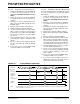
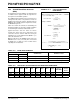
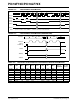
REGISTER 16-2: RCSTA: RECEIVE STATUS AND CONTROL REGISTER
R/W-0 R/W-0 R/W-0 R/W-0 R/W-0 R-0 R-0 R-x
SPEN RX9 SREN CREN ADDEN FERR OERR RX9D
bit 7 bit 0
Legend:
R = Readable bit W = Writable bit U = Unimplemented bit, read as ‘0’
-n = Value at POR ‘1’ = Bit is set ‘0’ = Bit is cleared x = Bit is unknown
bit 7 SPEN: Serial Port Enable bit
(1)
1 = Serial port enabled (configures RX/DT and TX/CK pins as serial port pins)
0 = Serial port disabled (held in Reset)
bit 6 RX9: 9-bit Receive Enable bit
1 = Selects 9-bit reception
0 = Selects 8-bit reception
bit 5 SREN: Single Receive Enable bit
Asynchronous mode
:
Don’t care
Synchronous mode – Master
:
1 = Enables single receive
0 = Disables single receive
This bit is cleared after reception is complete.
Synchronous mode – Slave:
Don’t care
bit 4 CREN: Continuous Receive Enable bit
Asynchronous mode:
1 = Enables receiver
0 = Disables receiver
Synchronous mode
:
1 = Enables continuous receive until enable bit CREN is cleared (CREN overrides SREN)
0 = Disables continuous receive
bit 3 ADDEN: Address Detect Enable bit
Asynchronous mode 9-bit (RX9 =
1):
1 = Enables address detection, enable interrupt and load the receive buffer when RSR<8> is set
0 = Disables address detection, all bytes are received and ninth bit can be used as parity bit
Asynchronous mode 8-bit (RX9 =
0):
Don’t care
Synchronous mode
:
Must be set to ‘0’
bit 2 FERR: Framing Error bit
1 = Framing error (can be updated by reading RCREG register and receive next valid byte)
0 = No framing error
bit 1 OERR: Overrun Error bit
1 = Overrun error (can be cleared by clearing bit CREN)
0 = No overrun error
bit 0 RX9D: Ninth bit of Received Data
This can be address/data bit or a parity bit and must be calculated by user firmware.
Note 1: The AUSART module automatically changes the pin from tri-state to drive as needed. Configure
TRISx = 1.