
Datasheet

PIC16F72X/PIC16LF72X
DS41341E-page 84 © 2009 Microchip Technology Inc.
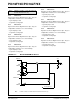
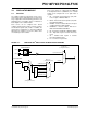
6.6 PORTE and TRISE Registers
PORTE
(1)
is a 4-bit wide, bidirectional port. The
corresponding data direction register is TRISE. Setting a
TRISE bit (= 1) will make the corresponding PORTE pin
an input (i.e., put the corresponding output driver in a
High-Impedance mode). Clearing a TRISE bit (= 0) will
make the corresponding PORTE pin an output (i.e.,
enable the output driver and put the contents of the
output latch on the selected pin). The exception is RE3,
which is input only and its TRIS bit will always read as
‘1’. Example 6-5 shows how to initialize PORTE.
Reading the PORTE register (Register 6-15) reads the
status of the pins, whereas writing to it will write to the
PORT latch. All write operations are read-modify-write
operations. Therefore, a write to a port implies that the
port pins are read, this value is modified and then
written to the PORT data latch. RE3 reads ‘0’ when
MCLRE = 1.
The TRISE register (Register 6-16) controls the PORTE
pin output drivers, even when they are being used as
analog inputs. The user should ensure the bits in the
TRISE register are maintained set when using them as
analog inputs. I/O pins configured as analog input always
read ‘0’.
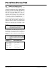
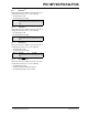
EXAMPLE 6-5: INITIALIZING PORTE
Note 1: RE<2:0> and TRISE<2:0> are not
implemented on the PIC16F722/723/726/
PIC16LF722/723/726. Read as ‘0’.
Note: The ANSELE register must be initialized to
configure an analog channel as a digital
input. Pins configured as analog inputs will
read ‘0’.
BANKSEL PORTE ;
CLRF PORTE ;Init PORTE
BANKSEL ANSELE ;
CLRF ANSELE ;digital I/O
BANKSEL TRISE ;
MOVLW B‘00001100’ ;Set RE<2> as an input
MOVWF TRISE ;and set RE<1:0>
;as outputs