
Datasheet

Installation and Operation
© 2011 Microchip Technology Inc. DS51999A-page 17
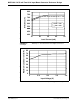
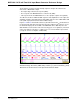
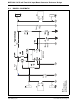
FIGURE 2-5: MCP1640 12V/50 mA Two Cells Input Boost Converter
Reference Design Test Points (SWH, SWL), Inductor (I
L
) and Load Current (I
OUT
)
Waveforms for 60 mA Load and 2.4V Input in Continuous mode.
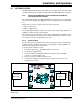
2.2.3 How Does the MCP1640 12V/50 mA Two Cells Input Boost
Converter Reference Design Works?
The board was designed to boost low voltage from two alkaline cells or NiCd/NiMH
cells to high voltage. The topology used in this reference design is adapting a
low-voltage boost converter into a high-voltage boost converter using a single inductor,
instead of using a flyback topology that requires a more expensive flyback transformer.
Another advantage is that the switching voltage spikes are kept below the safe value,
6V, for MCP1640 device’s SW pin.
The converter is configured as nonsynchronous; an external diode, D, is connected
between the inductor and the high-voltage output (V
OUT
).
The two sense resistors, R
T
and R
B
, set the output (V
OUT
) at 12.0V according to the
following equation:
EQUATION 2-1:
R
T
R
B
V
OUT
V
FB
-------------1–
⎝⎠
⎛⎞
×
=
Where:
V
FB
=1.21V
V
FB
= Reference voltage of the FB pin
V
OUT
= 12.0V
R
B
= Resistor’s value is selected by the designer
Note: The reference board is tested up to 24V output with a maximum load of
20 mA. The internal error amplifier is a transconductance type; its gain is
not related to the feedback resistors’ values.