Atmel AT30TSE002B Integrated Temperature Sensor with SEEPROM DATASHEET Features Integrated Temperature Sensor (TS) + 2-Kbit Serial EEPROM JEDEC (JC42.4) SO-DIMM SPD + TS compliant Standard voltage operation Optimized for voltage range: 2.7V to 3.
Figure 1. Pin Configuration Pin Function A0, A1, A2 Address Inputs SDA Serial Data SCL 1.
. Block Diagram Serial EEPROM Temperature Sensor Selected Resolution H.V Pump/Timing Temp.
. Pin Description AT30TSE002B requires no external components for operation except for pull-up resistors on SCL, SDA, and EVENT pins. In order to provide effective noise protection and filtering, it is recommended that a decoupling capacitor of 0.1F be used and is located as close as possible to the device between VCC and ground pins. Serial Clock (SCL): The SCL input is used to positive edge clock data into each EEPROM device and negative edge clock data out of each device.
Table 4-2. DC Characteristics Applicable over recommended operating range: TAI = –20°C to +125°C, VCC = +2.7v to +3.6V (unless otherwise noted) Symbol Parameter VCC1 Supply Voltage Test Condition Min Typ 2.7 Max Units 3.6 V Supply Current ICC EEPROM Read VCC = 3.6V (2) 100kHz 0.4 1.0 mA ICC EEPROM Write VCC = 3.6V (2) 100kHz 1.5 3.0 mA ICC Temp. Sensor VCC = 3.6V EEPROM Inactive 0.2 0.5 mA ICC Timeout Active VCC = 3.6V EEPROM Inactive, Temp. Sensor Shutdown 0.2 0.
Table 4-3. AC Characteristics Applicable over recommended operating range: TAI = –20°C to +125°C, VCC = +2.7v to +3.6V, CL = 1 TTL Gate and 100μF (unless otherwise noted) Symbol Parameter Min (2) Max Min Max Units 100 (2) 400 kHz FSCL Clock Frequency, SCL 10 TLOW Clock Pulse Width Low 4.7 1.2 us THIGH Clock Pulse Width High 4.0 0.6 us TR Inputs Rise Time(1) (1) 10 1.0 0.3 us 300 300 ns TF Inputs Fall Time TSU.DAT Data In Set-up Time THD.DI Data In Hold Time THD.
5. Memory Organization AT30TSE002B, 2K Serial EEPROM: The 2K memory is internally organized with 16 pages of 16-bytes each. Random word addressing requires an 8-bit data word address. 6. Device Operation Clock and Data Transitions: The SDA pin is normally pulled high with an external device. Data on the SDA pin may change only during SCL low time periods. (See Figure 6-4) Data changes during SCL high periods will indicate a start or stop condition as defined below.
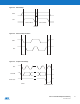
Figure 6-2. Bus Timing SCL Serial Clock SDA: Serial Data I/O tHIGH tLOW SCL tHD:STA tBUF tSU:STO SDA IN tSU:STA SDA Input tHD:DI SDA Change tSU:DAT STOP Condition START Condition SCL tHD:DAT SDA OUT Data Valid Figure 6-3.
Figure 6-4. Data Validity SDA SCL DATA STABLE DATA STABLE DATA CHANGE Figure 6-5. Start and Stop Condition SDA SCL START STOP Figure 6-6.
7. Device Addressing AT30TSE002B device requires an 8-bit device address word following a start condition to enable the chip to access either the Temperature Sensor or EEPROM functions (See Table 7-1). Table 7-1. Control/Device Address Word Control / Device Address Word Device ID Device Device Address Bits B7 B6 B5 B4 EEPROM 1 0 1 0 Temperature Sensor 0 0 1 1 EEPROM Write Protection 0 1 1 0 Note: 1.
9. EEPROM Write Protection The device supports permanent and reversible software write protection and once enabled, write protects the first-half of the array (00H - 7FH). Permanent Software Write Protection: The software write protection is enabled by sending a command similar to a normal write command; to the device which programs the permanent write protect register.
10.3 Temperature Sensor Power-on Default The AT30TSE002B has an internal Power-On Reset (POR) circuit. When the supply voltage drops below the POR threshold, the device will reset to the following power-on default conditions: 10.4 Sensor starts monitoring temperature continuously. Address Pointer Register = 00h. Upper / Lower Alarm Trip registers and Crit_Alarm registers are set to 0°C. EVENT register cleared and pulled high by external pull up resistor. Operational mode is comparator.
11. Register Descriptions This section describes all the temperature sensor registers that are used in AT30TSE002B. The AT30TSE002B has several registers that are user accessible and or programmable and used for latching temperature readings, storing high and low temperature limits, configuring the hysteresis threshold and reporting status.
11.1 Address Pointer Register The AT30TSE002B uses a Pointer Register to select and access the 16-bit data registers shown in Table 11-1. The Pointer Register is an 8-bit write only register (See Table 11-2). The power-on default value is 00h which is the address location for the capability register. Table 11-2. Address Pointer Register Bit 7 6 5 4 Symbol 11.
Table 11-4. Capability Register Bit Description Bit 15:8 Symbol Description RFU Reserved for Future Use. Must be zero. Event Output Status during shutdown mode: 7 EVSD 1 = The EVENT pin output is deasserted (not driven) when entering shutdown mode and will resume status update immediately upon exiting shutdown. In addition, the EVTSTS bit in the configuration register will be cleared when entering shutdown mode and will resume status update immediately upon exiting shutdown.
Table 11-6. Configuration Register Bit Description Bit 15:11 Symbol Description RFU Reserved for Future Use and must be zero. Hysteresis Enable: 00 = 0°C Disable Hysteresis (default power-on condition) 01 = 1.5°C Enable Hysteresis 10 = 3.0°C Enable Hysteresis 11 = 6.0°C Enable Hysteresis 10:9 HYSTENB The purpose of these bits is to control the hysteresis applied to the alarm trip point boundaries.
Table 11-6. Configuration Register Bit Description (Continued) Bit Symbol Description EVENT Pin Output Status: 0 = The EVENT Output is not asserted by the device (power-on default). 4 EVTSTS 1 = The EVENT Output is asserted due to an alarm trip condition. Note: This bit will be cleared when entering shutdown mode and will resume status update immediately upon exiting shutdown. EVENT Output Control: This bit, when set, prevents the EVENT pin from generating an interrupt.
To remedy this ambiguity in the TSE2002av specification, one must avoid setting both bit two and three of the Configuration register to Logic 1 concurrently. Instead, bit two should be set first before bit three in separate commands to offer universal compatibility if the system is designed to only trigger off the Critical Alarm temperature threshold. Please see the Atmel Application Note, “Utilizing a Digital Temperature Sensor in a DDR3 DIMM,” for more details. Figure 11-1.
11.4 Upper Alarm Trip Register (16-bit Read/Write, Address = 02h) The Upper Alarm Trip Register holds the user programmed upper temperature boundary trip point in 11-bit twos complement format (0.25°C resolution) that can be used to monitor ambient temperature in an operating window (See Table 11-7 and Table 11-8). When the temperature increases above this trip point, or drops below, or is equal to the trip point (minus any hysteresis set), then the EVENT pin is asserted (if enabled).
11.5 Lower Alarm Trip Register (16-bit Read/Write, Address = 03h) The Lower Alarm Trip Register holds the user programmed lower temperature boundary trip point in 11-bit twos complement format (0.25°C resolution) that can be used to monitor ambient temperature in an operating window (See Table 11-9 and Table 11-10). When temperature decreases below this trip point minus any hysteresis set or increases to meet or exceed this trip point, then the EVENT pin is asserted (if enabled).
11.6 Critical Alarm Trip Register (16-bit Read/Write, Address = 04h) The Critical Alarm Trip Register holds the user programmed Critical Alarm temperature boundary trip point in 11-bit twos complement format (0.25°C resolution) that can be used to monitor ambient temperature (See Table 11-11 and Table 11-12). When the temperature increases above this trip point, the EVENT pin will be asserted (if enabled).
11.7 Temperature Register (16-bit Read-only, Address = 05h) The Temperature Register holds the internal temperature measurement data represented in 11-bit twos complement word format allowing for resolution equal to 0.125°C (least significant bit). The upper three bits (15, 14, and 13) of the temperature register indicates the trip status of the current temperature and most important, are not affected by the status of the output of the EVENT pin (See Table 11-13 and Table 11-14). Table 11-13.
11.7.1 Temperature Register Format This section will clarify the temperature register format and temperature bit value assignments used for temperature for the following registers: Upper Alarm Trip, Lower Alarm Trip, Critical Alarm Trip, and Temperature Data Registers. The temperatures expressed in the Upper Alarm Trip, Lower Alarm Trip, Critical Alarm Trip, and Temperature Data Registers are indicated in twos complement format.
11.8 Manufacturer ID Register (16-bit Read-only, Address = 06h) This register is used to identity the manufacturer of the product. The manufacturer ID for the AT30TSE002B is 001Fh (See Table 11-17). Table 11-17. Manufacturer ID Register Bit Distribution Bit 15 14 13 Symbol 11 10 9 8 Manufacturer ID Default Value 0 0 0 0 0 0 0 0 R / W access R R R R R R R R 7 6 5 4 3 2 1 0 Bit Symbol 11.
11.10 SMBus Register (16-bit Write/Read only, Address = 22h) The SMBus Register allows the user to enable or disable the SMBus time out feature (See Table 11-19 and Table 11-20). Table 11-19. SMBus Register Bit Distribution Bit 15 14 13 12 Symbol 11 10 9 8 RFU Default Value 0 0 0 0 0 0 0 0 R / W access R R R R R R R R 7 6 5 4 3 2 1 0 Bit Symbol SMBOUT RFU Default Value 0 0 0 0 0 0 0 0 R / W access R/W R R R R R R R Table 11-20.
12. TS Write Operations Writing to the AT30TSE002B Temperature register set is accomplished through a modified write operation for two data bytes. To maintain 2-wire compatibility, the 16-bit register is accessed through a pointer register, requiring the write sequence to include an address pointer in addition to the device address. This indicates the storage location for the next two bytes received. Table 12-1 shows an entire write transaction on the bus. Figure 12-1.
Figure 12-4. 2-wire Pointer Write Register Word Read S T A R T W R I T E Device Address 0 0 1 S T A R T Register Pointer 1 A2 A1 A0 Device Address 0 R A / C W K 0 1 R E A D Data MSB S T O P Data LSB 1 A2 A1 A0 A C K R A / C W K A C K N O A C K Figure 12-5. Setting Permanent Write Protect Register (PSWP) S T A R T SDA Line Control Byte Word Address S T O P Data 0 1 1 0 A2 A1 A0 0 A C K A C K A C K = Dummy bit Figure 12-6.
Table 12-1. EEPROM Write Protection Pin Preamble R/W Command A2 A1 A0 B7 B6 B5 B4 B3 B2 B1 B0 Set PSWP A2 A1 A0 0 1 1 0 A2 A1 A0 0 Set RSWP 0 0 VHV 0 1 1 0 0 0 1 0 Clear RSWP 0 1 VHV 0 1 1 0 0 1 1 0 Min Max Units 7 10 V Table 12-2. VHV VHV Table 12-3.
13. EEPROM Read Operations Read operations are initiated the same way as write operations with the exception that the read/write select bit in the device address word is set to one. There are three read operations: current address read, random address read, and sequential read. Current Address Read: The internal data word address counter maintains the last address accessed during the last read or write operation, incremented by one.
Figure 13-2. EEPROM Byte Write S T A R T Device Address W R I T E Word Address S T O P Data SDA Line M S B R A / C W K M S B A C K A C K Figure 13-3. EEPROM Page Write S T A R T Device Address W R I T E Word Address (n) Data (n) Data (n + 1) S T O P Data (n + x) SDA Line M S B L R A S / C B W K A C K A C K A C K A C K Figure 13-4.
Figure 13-5. EEPROM Random Read S T A R T Device Address W R I T E S T A R T Word Address (n) R E A Device Address D S T O P Data (n) SDA Line M S B L R A S / C B W K M S B L A S C B K M S B L S B A C K N O A C K Dummy Write Figure 13-6.
14. Part Marking 14.1 WDFN Marking AT30TSE002B: Package Marking Information 8-lead UDFN 2.0 x 3.0 mm Body T2B H2@ YXX Note 1: designates pin 1 Note 2: Package drawings are not to scale Catalog Number Truncation AT30TSE002B Truncation Code: T2B Date Codes Y = Year 2: 2012 3: 2013 4: 2014 5: 2015 Voltages 6: 2016 7: 2017 8: 2018 9: 2019 M = Month A: January B: February ... L: December WW = Work Week of Assembly 02: Week 2 04: Week 4 ...
15. Ordering Information 15.1 Ordering Code Detail AT 3 0 T S E 0 0 2 B - M A H - T Shipping Carrier Option Atmel Designator B = Bulk (tubes) T = Tape and reel Product Family Device Grade H = Green, NiPdAu lead finish Temperature range (-20°C to +125°C) Memory Type E = EEPROM Package Option Sensor Type MA = 8-lead, 2 x 3 x 0.8mm (WDFN) Device Density 2 = 2-kilobit Device Revision 15.2 Green Package Options (Pb/Halide-free/RoHS Compliant) Ordering Code AT30TSE002B-MAH-T Note: 1.
16. Package Drawings 16.1 8M2 – 8-lead WDFN D2 A b (8X) E E2 Pin 1 Index Area Pin 1 ID L (8X) D e (6X) A1 1.50 REF. COMMON DIMENSIONS (Unit of Measure = mm) A3 SYMBOL MIN D 2.00 BSC E 3.00 BSC D2 1.35 1.40 1.45 E2 1.25 1.30 1.35 A 0.70 0.75 0.80 A1 0.0 0.02 0.05 A3 L b NOTE 0.20 REF 0.35 e Notes: MAX NOM 0.40 0.45 0.50 BSC 0.18 0.25 0.30 2 1. This drawing is for general information only.
17. Revision History Doc. Rev. 8711G Date 05/2012 Comments Add JEDEC TSE2002av compliant paragraphs after the Configuration Register Bit Description table. Update template. 8711F 03/2011 WDFN marking added “2” and @ = location of assembly. Update Table, “Register Summary,” 00D7h to 00F7H. 8711E 12/2010 Correct cross reference in EEPROM Write Protection and TS WRITE Operations sections. Change note under Green Package Options table. Update R to R / W for 22h in Register Summary table.
Atmel Corporation 2325 Orchard Parkway Atmel Asia Limited Unit 01-5 & 16, 19F Atmel Munich GmbH Business Campus Atmel Japan G.K. 16F Shin-Osaki Kangyo Bldg San Jose, CA 95131 BEA Tower, Millennium City 5 Parkring 4 1-6-4 Osaki, Shinagawa-ku USA 418 Kwun Tong Roa D-85748 Garching b. Munich Tokyo 141-0032 Tel: (+1) (408) 441-0311 Kwun Tong, Kowloon GERMANY JAPAN Fax: (+1) (408) 487-2600 HONG KONG Tel: (+49) 89-31970-0 Tel: (+81) (3) 6417-0300 www.atmel.